Document
advertisement
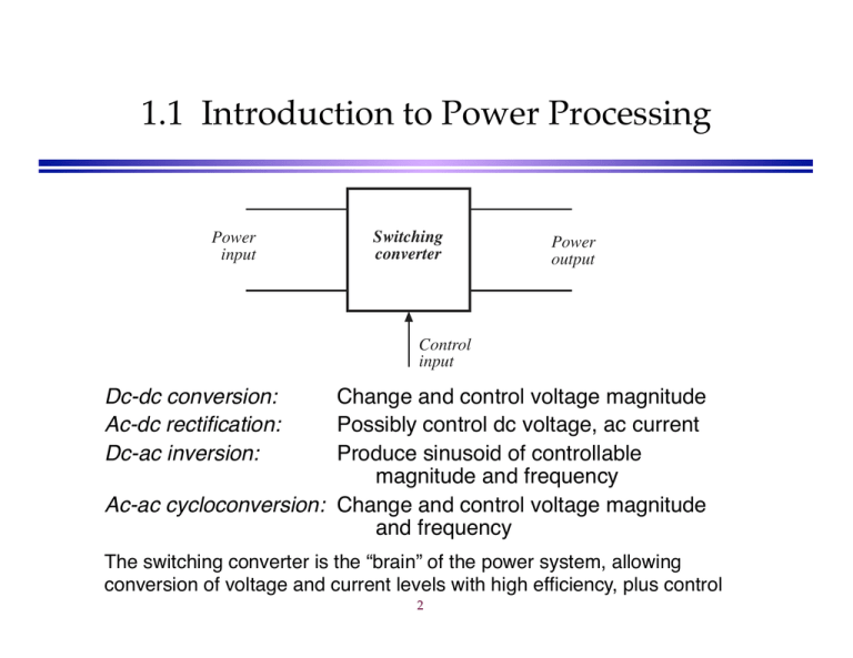
1.1 Introduction to Power Processing! Power input Switching converter Power output Control input Dc-dc conversion: Ac-dc rectification: Dc-ac inversion: !Change and control voltage magnitude! !Possibly control dc voltage, ac current! !Produce sinusoid of controllable magnitude and frequency! Ac-ac cycloconversion: !Change and control voltage magnitude and frequency! The switching converter is the “brain” of the power system, allowing conversion of voltage and current levels with high efficiency, plus control! 2! Control is invariably required! Power input Switching converter Power output Control input Feedforward Feedback Controller Reference 3! • Traditional analog feedback! • Sophisticated control using inexpensive digital microcontrollers! High Efficiency is Essential! = Pout Pin Ploss = Pin – Pout = Pout 1 – 1 • High efficiency leads to low power loss within converter • Small size and reliable operation is then feasible • A good measure of converter performance is the ratio of output power to loss: Pout = Ploss 1 – Converters generally are losslimited, and technologies that can produce large output power while incurring small loss result in small size and low cost Pin Converter Large input power 10! Small converter Pout Large output power + – Devices available to the circuit designer! DT Resistors Capacitors Magnetics 11! T s s Linearmode Switched-mode Semiconductor devices + – Devices available to the circuit designer! DT Resistors Capacitors Magnetics Signal processing: avoid magnetics! 12! T s s Linearmode Switched-mode Semiconductor devices + – Devices available to the circuit designer! DT Resistors Capacitors Magnetics Power processing: avoid lossy elements! 13! T s s Linearmode Switched-mode Semiconductor devices Power loss in an ideal switch! 1 Switch closed: !v(t) = 0 Switch open: + !i(t) = 0 In either event: !p(t) = v(t) i(t) = 0! i v – Ideal switch consumes zero power! 14! 0 A simple dc-dc converter example! I 10 A + Vg 100 V + – Dc-dc converter R 5 V 50 V – Input source: 100V! Output load: 50V, 10A, 500W! How can this converter be realized?! 15! Dissipative realization! Resistive voltage divider! I 10 A + Vg 100 V + – + 50 V – Ploss = 500 W R 5 V 50 V – Pin = 1000 W Pout = 500 W 16! Dissipative realization! Series pass regulator: transistor operates in active region! I 10 A + 50 V – + Vg 100 V + – Linear amplifier and base driver Ploss 500 W –+ Vref R 5 V 50 V – Pin 1000 W Pout = 500 W 17! Use of a SPDT switch! I 10 A 1 + Vg 100 V + 2 + – vs(t) R – vs(t) – Vg Vs = DVg switch position: DTs 0 (1 – D) Ts t 1 2 1 18! v(t) 50 V The switch changes the dc voltage level! vs(t) Vg Vs = DVg switch position: DTs 0 (1 – D) Ts t 1 2 1 DC component of vs(t) = average value:! 19! D = switch duty cycle! !0 ≤ D ≤ 1 Ts = switching period! ! fs = switching frequency! = 1 / Ts Addition of low pass filter! Addition of (ideally lossless) L-C low-pass filter, for removal of switching harmonics:! i(t) 1 + Vg 100 V + – + L 2 vs(t) C – Pin 500 W Ploss small R v(t) – Pout = 500 W • Choose filter cutoff frequency f0 much smaller than switching frequency fs • This circuit is known as the “buck converter”! 20! Addition of control system" for regulation of output voltage! Power input Switching converter Load + + – v H(s) – Transistor gate driver Error signal ve Pulse-width vc G (s) c modulator Compensator (t) dTs Ts –+ vg i Reference vref input t 21! Hv Sensor gain The boost converter! 2 + L Vg 1 + – C R V – 5Vg 4Vg V 3Vg 2Vg Vg 0 0 0.2 0.4 0.6 D 22! 0.8 1 A single-phase inverter! 1 Vg + – vs(t) + – + v(t) 2 – 2 1 Load vs(t) “H-bridge”! t 23! Modulate switch duty cycles to obtain sinusoidal low-frequency component!
