Application Note: Virtex-II, Virtex-II Pro, Virtex-4, Virtex-5,
Spartan-3, and Spartan-3E Families
Connecting Devices in the Virtex and
Spartan Families to a 3.3V or 5V PCI Bus
R
XAPP646 (v1.2.2) April 23, 2007
Summary
This application note describes how to connect Virtex™-II, Virtex-II Pro, Virtex-4, Virtex-5,
Spartan™-3, and Spartan-3E devices to 3.3V or 5V PCI buses. The design responds to
customer demand for a general solution for applications with a Virtex-II device and a 5V PCI
bus, as well as for applications with a Virtex-II Pro, Virtex-4, Virtex-5, Spartan-3, or Spartan-3E
device and a 3.3V or 5V PCI bus.
3.3V/5V
Universal PCI
Implementation
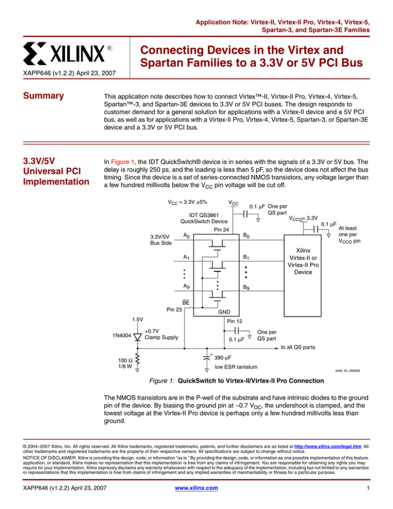
In Figure 1, the IDT QuickSwitch® device is in series with the signals of a 3.3V or 5V bus. The
delay is roughly 250 ps, and the loading is less than 5 pF, so the device does not affect the bus
timing. Since the device is a set of series-connected NMOS transistors, any voltage larger than
a few hundred millivolts below the VCC pin voltage will be cut off.
VCC = 3.3V ±5%
VCC
0.1 μF One per
QS part
IDT QS3861
QuickSwitch Device
VCCO= 3.3V
Pin 24
3.3V/5V
Bus Side
A0
B0
A1
B1
A9
B9
0.1 μF
At least
one per
VCCO pin
Xilinx
Virtex-II or
Virtex-II Pro
Device
BE
Pin 23
GND
1.5V
1N4004
Pin 12
+0.7V
Clamp Supply
0.1 μF
One per
QS part
to all QS parts
100 Ω
1/8 W
+
390 μF
low ESR tantalum
x646_04_080602
Figure 1: QuickSwitch to Virtex-II/Virtex-II Pro Connection
The NMOS transistors are in the P-well of the substrate and have intrinsic diodes to the ground
pin of the device. By biasing the ground pin at ~0.7 VDC, the undershoot is clamped, and the
lowest voltage at the Virtex-II Pro device is perhaps only a few hundred millivolts less than
ground.
© 2004–2007 Xilinx, Inc. All rights reserved. All Xilinx trademarks, registered trademarks, patents, and further disclaimers are as listed at http://www.xilinx.com/legal.htm. All
other trademarks and registered trademarks are the property of their respective owners. All specifications are subject to change without notice.
NOTICE OF DISCLAIMER: Xilinx is providing this design, code, or information "as is." By providing the design, code, or information as one possible implementation of this feature,
application, or standard, Xilinx makes no representation that this implementation is free from any claims of infringement. You are responsible for obtaining any rights you may
require for your implementation. Xilinx expressly disclaims any warranty whatsoever with respect to the adequacy of the implementation, including but not limited to any warranties
or representations that this implementation is free from claims of infringement and any implied warranties of merchantability or fitness for a particular purpose.
XAPP646 (v1.2.2) April 23, 2007
www.xilinx.com
1
R
Connecting Devices in the Virtex and Spartan Families to a 3.3V or 5V PCI Bus
The B side of the QuickSwitch device will limit the positive overshoot voltage from the A side to
less than ~3.0V, and also limit the negative undershoot excursions to not more than –0.1 volt.
The 0.1 μF bypass capacitor from VCC to ground (one each per QuickSwitch device), and the
0.1 μF bypass capacitor from the ground pin bias point to the system ground are required to
absorb the transients and provide a good clamping and cutoff action.
The 0.7V bias supply is easily generated by a forward biased diode from the VCCINT 1.5V
supply. A large tantalum (or low ESR aluminum electrolytic) may be required to keep this
voltage stable over all possible bus activity duty cycles. The pull-down resistor sets the
maximum bias supply voltage at ~0.9V DC. Up to four QuickSwitch devices can be biased from
this supply to support the 66/64-bit PCI bus, for example.
The undershoot current is roughly 10 mA average per pin, so that the supply with the 1A diode
easily can provide the necessary current (about 0.66A, worst case).
Bypassing the Virtex or Spartan device at less than 35 mm (<1.4 inches) is also key to
providing a good interface.
NOTE: This reference design has been verified to work in PCI systems. However, it will not meet one
of the PCI compliance requirements because the PCI signal loading specification does not allow pullup resistors or external devices (in this case, the bus switch) attached to PCI signals. Check your PCI
design compliance goals before using this reference design. See XAPP653 for an alternative solution
that does not use an external bus switch.
For more information about the Xilinx implementation of the PCI standard, refer to the Virtex-II
or Virtex-II Pro User Guides and other Xilinx documentation.
IDT QuickSwitch Technology
In its basic form, the QuickSwitch technology is an N-channel FET switch controlled by either
combinatorial or sequential control logic using CMOS technology. Figure 2 shows the basic
QuickSwitch configuration.
A0
B0
A9
B9
BE
x646_05_080602
Figure 2: Basic QuickSwitch Configuration
When the switch is enabled, the gate of the N-channel switch transistor driven by a CMOS logic
gate is at VCC and the switch exhibits a typical ON resistance of 5Ω. The series resistance will
be higher than 5Ω when VCC supply is 3.3V and port A is driven by 5V. Consider the QS3R861
if a lower ON resistance is desired. When disabled, the gate of the switch is at ground potential
and the switch offers very high resistance between the A and B terminals. In the OFF state, the
leakage current at the switch terminals is typically 10 nA, and the capacitance between the
terminals is low. Typical capacitance at the switch terminals is 5 pF in the OFF state.
XAPP646 (v1.2.2) April 23, 2007
www.xilinx.com
2
R
Connecting Devices in the Virtex and Spartan Families to a 3.3V or 5V PCI Bus
QuickSwitch devices are available from IDT with an estimated 1K volume price of about $0.30
each for the SO and Q packages, and $0.75 for the PA package. Table 1 shows the part
numbers and dimensions of each package.
Table 1: QuickSwitch Package Information
Part Number
Length x Width x Thickness (mm)
IDTQS3861SO (Small-Outline Package)
15.4 x 7.5 x 2.34
IDTQS3861Q (Quarter Size Outline Package)
8.7 x 3.8 x 1.47
IDTQS3861PA (Thin-Shrink Small-Outline Package)
7.8 x 4.4 x 1.0
For more information on QuickSwitch devices, refer to http://www.idt.com.
Revision
History
The following table shows the revision history for this document.
XAPP646 (v1.2.2) April 23, 2007
Date
Version
Revision
06/17/02
1.0
Initial Xilinx release.
08/01/02
1.1
Revised Figure 1 for clarification.
08/08/02
1.2
Revised Figure 1 for clarification, revised text with regards to
QuickSwitch devices.
01/16/04
1.2.1
Added paragraph on page 2 noting non-compliance with PCI signal
loading specification.
04/23/07
1.2.2
•
Expanded the menu of device families to which this application
note is applicable: Virtex-II, Virtex-II Pro, Virtex-4, Virtex-5,
Spartan-3, and Spartan-3E families.
•
Changed title.
www.xilinx.com
3


