Technical Note
HIGH PERFORMANCE EMCCD & CCD CAMERAS FOR LIFE SCIENCES
Keep the Noise Down!
Low Noise: An Integral Part of High-Performance
CCD (HCCD) Camera Systems
Noise is composed of undesirable signal components that
arise from various sources in an electronic imaging system.
The figure of merit that dictates the ultimate performance of
a system is signal-to-noise ratio (SNR), which describes the
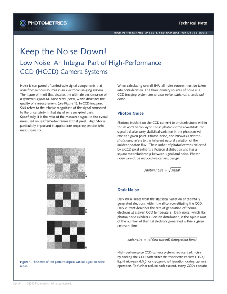
quality of a measurement (see Figure 1). In CCD imagine,
SNR refers to the relative magnitude of the signal compared
to the uncertainty in that signal on a per-pixel basis.
Specifically, it is the ratio of the measured signal to the overall
measured noise (frame-to-frame) at that pixel. High SNR is
particularly important in applications requiring precise light
measurements.
When calculating overall SNR, all noise sources must be taken
into consideration. The three primary sources of noise in a
CCD imaging system are photon noise, dark noise, and read
noise.
Photon Noise
Photons incident on the CCD convert to photoelectrons within
the device’s silicon layer. These photoelectrons constitute the
signal but also carry statistical variation in the photo arrival
rate at a given point. Photon noise, also known as photonshot noise, refers to the inherent natural variation of the
incident photon flux. The number of photoelectrons collected
by a CCD pixel exhibits a Poisson distribution and has a
square root relationship between signal and noise. Photon
noise cannot be reduced via camera design.
Dark Noise
Dark noise arises from the statistical variation of thermally
generated electrons within the silicon constituting the CCD.
Dark current describes the rate of generation of thermal
electrons at a given CCD temperature. Dark noise, which like
photon noise exhibits a Poisson distribution, is the square root
of the number of thermal electrons generated within a given
exposure time.
Figure 1. This series of test patterns depicts various signal-to-noise
ratios.
Rev A1
©2010 Photometrics. All rights reserved.
High-performance CCD camera systems reduce dark noise
by cooling the CCD with either thermoelectric coolers (TECs),
liquid nitrogen (LN2), or cryogenic refrigeration during camera
operation. To further reduce dark current, many CCDs operate
1
Low Noise: An Integral Part of High-Performance CCD Camera Systems
in multi-pinned-phase (MPP) mode. The largest contribution
to dark current results from the interface between the silicon
dioxide and the epitaxial silicon layer within the CCD. MPP
devices are fabricated and operated in such a way as to
significantly reduce this source of thermal charge generation.
In practical terms, the noise arising from dark current should
be reduced by cooling the CCD to a point at which its
contribution is negligible over a typical exposure time.
Read Noise
Electronic noise sources inherent to the camera system and
the CCD also introduce uncertainty in the measured signal.
Collectively these noise components are referred to as read
noise and represent the error introduced during the process
of quantifying the electronic signal on the CCD. The major
component of read noise arises from the on-chip preamplifier.
Spurious charge also contributes to the overall read noise of
the imaging system.
Technical Note
Photometrics can provide quantum efficiency, dark current,
and read noise parameters for each CCD, camera head,
and digitization rate offered. If the incident light levels are
known, these parameters can be used to determine the SNR
for any Roper Scientific camera system. Note that because
incident photon flux, background photon flux, and quantum
efficiency are each a function of wavelength, Equation 1 must
be integrated over all wavelengths of interest when a CCD is
exposed to a broad-band radiation source. Under low-lightlevel conditions, read noise exceeds photon noise and the
image data is said to be read-noise limited. The integration
time can be increased until photon noise exceeds both read
noise and dark noise. At this point the image is said to be
photon-noise limited.
HCCD camera systems are able to lower read noise by
employing carefully designed electronics. For instance, to
lessen CCD preamplifier noise, CCD designers employ the
latest advances in high-resolution photolithography to
reduce the feature sizes of on-chip amplifiers, a step that
directly reduces capacitance and thus allows more sensitivity.
Additionally, dual-slope integrators or correlated double
sampling methods are used to filter out specific components
of read noise, such as kTC noise and 1/f noise.
The signal-to-noise ratio for a CCD camera can be calculated
as follows:
Equation 1
P =
B =
Qe =
t =
D =
Nr =
Rev A1
photon flux incident on the CCD
(photons/pixel/second)
background photo flux incident on the CCD
(photons/pixel/second) — background light can
arise from many sources and is usually scattered light
that is not of interest to the observer — when the
signal is the only source of light, B equals 0
quantum efficiency of the CCD
integration time (seconds)
dark current (electrons/pixel/second) — as
discussed earlier, dark noise equals the square
root of Dt
read noise (electrons rms/pixel)
©2010 Photometrics. All rights reserved.
Figure 2. Under low-light-level conditions, high-performance
CCD camera systems become photon-noise limited at shorter
exposure times.
Figure 2 plots the SNR as a function of exposure time using
Equation 1 with parameters typical of a high-performance
camera designed for low-light-level imaging applications. In
this example, read noise is the dominant noise source for short
exposure times. For this region of the graph, Equation 1 can
be simplified as shown in Equation 2.
Equation 2
2
Low Noise: An Integral Part of High-Performance CCD Camera Systems
Technical Note
Figure 3. The charge from adjacent pixels in a CCD can be combined
during readout to improve the signal-to-noise ratio. Note that the
higher SNR comes at the expense of spatial resolution.
The detected photon signal increases with longer exposure
times, which in turn makes photon noise the dominant
noise source. For this region of the graph, Equation 1 can be
simplified to Equation 3.
square root of the number of exposures – in this instance,
by about a factor of three when ten 0.1-second exposures
are taken. Thus, one long exposure (on-chip integration) is
better than many short exposures (frame averaging) in the
read-noise-limited region.
Equation 3
Now consider the difference between ten exposures of
10-seconds duration and a single 100-second exposure. In
the photon-noise-limited region, the SNR increases only as
the square root of the exposure time – so both techniques
give essentially the same SNR. There are other factors that
should also be taken into account though, such as the effects
of cosmic rays. Because cosmic rays do not impact the same
pixels on multiple frames, these events can readily be removed
from the sum by comparing the frames. Meanwhile, it can
be very difficult to remove the effects of cosmic rays from a
single frame, especially if there are point sources in the image
that can be confused with these events.
In Figure 2, the points computed using Equation 1 are
represented by boxes. Notice that Equation 2 (the solid line)
fits the computed points for shorter exposure times, while
Equation 3 (the dashed line) fits the computed points for
longer exposure times. The intersection of Equations 2 and 3
divide the graph into two sections, a read-noise-limited region
and a photon-noise-limited region.
When imaging, it should be taken into consideration whether
there is a difference in SNR if many short exposures are
acquired and then added together, or if a single long exposure
is acquired for that total length of time. The same number of
photons is collected in either case, but the strategies for image
optimization are different in the two regions of the graph.
The SNR increases linearly with time if the mean pixel value
is within the read-noise-limited region. A single 1.0-second
exposure has about ten times the SNR of a single
0.1-second exposure in this region. Adding together the
multiple exposures, however, will increase the SNR by the
Rev A1
©2010 Photometrics. All rights reserved.
An alternative means of raising the SNR is to use a technique
known as on-chip binning. On-chip binning is the process of
combining charge from adjacent pixels of a CCD array during
readout into a single superpixel (see Figure 3). Consolidating
the detected charge by binning neighboring pixels may allow
a system to reach a photon-noise-limited signal more quickly
(see Figure 4), with an inherent trade-off in spatial resolution.
On-chip binning also increases the dark current per superpixel
by the same factor.
Equation 1 can be modified to include binning, as shown in
Equation 4, where M represents the number of binned pixels.
Note that this equation assumes that the signal in each pixel is
the same.
3
Low Noise: An Integral Part of High-Performance CCD Camera Systems
Technical Note
Figure 4. Binning can improve the SNR of a device, allowing the
imaging system to reach a photon-noise-limited signal more quickly.
Equation 4
High-performance CCD camera systems are designed
specifically to be photon-noise limited at lower signal levels.
In other words, by reducing read noise and dark noise,
HCCD camera systems achieve higher signal-to-noise ratios
and reach optimal noise-performance territory faster than
other imaging systems – some of which never operate in the
photon-noise-limited region under low-light-level conditions.
In conclusion, HCCD digital imaging system designs provide
the high signal-to-noise ratios necessary for low-light-level
applications. High-performance CCD camera systems
also offer the flexibility to employ a wide range of imageacquisition strategies in order to optimize noise performance
for any given set of conditions.
USA 520.889.9933
Asia Pacific +65.6841.2094
Rev A1
France +33.1.60.86.03.65
Germany +49.89.660.779.3
©2010 Photometrics. All rights reserved.
Japan +81.3.5639.2731
UK +44.1628.890858
www.photometrics.com
info@photometrics.com
4


