PA3-110 - HRL Laboratories
advertisement
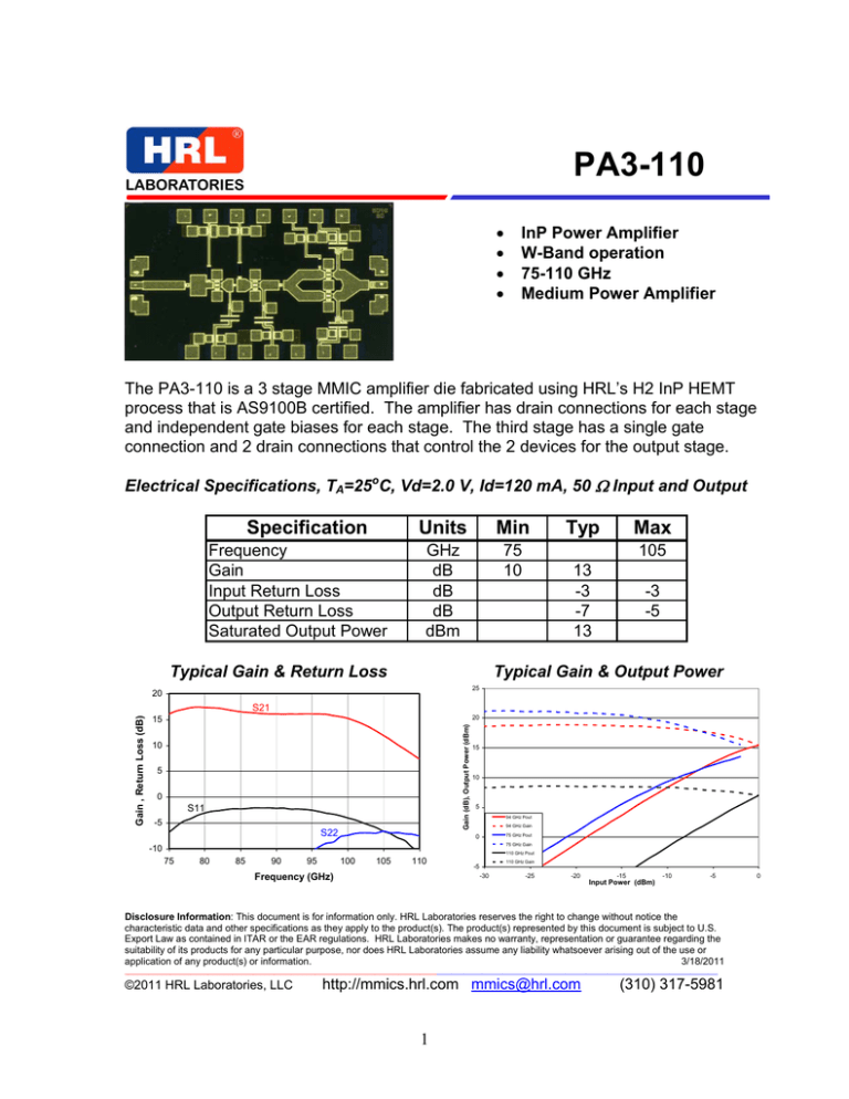
PA3-110 InP Power Amplifier W-Band operation 75-110 GHz Medium Power Amplifier The PA3-110 is a 3 stage MMIC amplifier die fabricated using HRL’s H2 InP HEMT process that is AS9100B certified. The amplifier has drain connections for each stage and independent gate biases for each stage. The third stage has a single gate connection and 2 drain connections that control the 2 devices for the output stage. Electrical Specifications, TA=25oC, Vd=2.0 V, Id=120 mA, 50 Input and Output Specification Frequency Gain Input Return Loss Output Return Loss Saturated Output Power Units Min GHz dB dB dB dBm 75 10 Typical Gain & Return Loss Typ Max 105 13 -3 -7 13 -3 -5 Typical Gain & Output Power 25 20 20 Gain (dB), Output Power (dBm) Gain , Return Loss (dB) S21 15 10 5 0 S11 -5 S22 15 10 5 94 GHz Pout 94 GHz Gain 75 GHz Pout 0 75 GHz Gain -10 110 GHz Pout 75 80 85 90 95 100 105 110 110 GHz Gain -5 -30 Frequency (GHz) -25 -20 -15 -10 -5 Input Power (dBm) Disclosure Information: This document is for information only. HRL Laboratories reserves the right to change without notice the characteristic data and other specifications as they apply to the product(s). The product(s) represented by this document is subject to U.S. Export Law as contained in ITAR or the EAR regulations. HRL Laboratories makes no warranty, representation or guarantee regarding the suitability of its products for any particular purpose, nor does HRL Laboratories assume any liability whatsoever arising out of the use or application of any product(s) or information. 3/18/2011 ___________________________________________________________________________________________________________________________________________________________________________ ©2011 HRL Laboratories, LLC http://mmics.hrl.com mmics@hrl.com 1 (310) 317-5981 0 Table I Maximum Ratings Symbol Parameter Value PIN Input Power 10 dBm VDS Drain to Source Voltage 2.0 V VGD Gate to Drain Voltage -2.5 to 0.0 VDC VGS Gate to Source Voltage -1.0 to 0.0 VDC TM Die Attach Temperature (30 seconds) 290o C Note Outline Drawing Bond pads are nominally 0.1 mm square Bond pad locations shown from die edge to pad center Die thickness is nominally 50 um Solid models and CAD files available at http://mmics.hrl.com Disclosure Information: This document is for information only. HRL Laboratories reserves the right to change without notice the characteristic data and other specifications as they apply to the product(s). The product(s) represented by this document is subject to U.S. Export Law as contained in ITAR or the EAR regulations. HRL Laboratories makes no warranty, representation or guarantee regarding the suitability of its products for any particular purpose, nor does HRL Laboratories assume any liability whatsoever arising out of the use or application of any product(s) or information. 3/18/2011 ___________________________________________________________________________________________________________________________________________________________________________ ©2011 HRL Laboratories, LLC http://mmics.hrl.com mmics@hrl.com 2 (310) 317-5981 DC Schematic GND VG1 GND VG2 GND VG3 VD3 GND 1 2 1 RF Input GND RF Output 2 1 1 2 VD1 GND 2 GND VD2 GND VD3 Typical Assembly Drawing Disclosure Information: This document is for information only. HRL Laboratories reserves the right to change without notice the characteristic data and other specifications as they apply to the product(s). The product(s) represented by this document is subject to U.S. Export Law as contained in ITAR or the EAR regulations. HRL Laboratories makes no warranty, representation or guarantee regarding the suitability of its products for any particular purpose, nor does HRL Laboratories assume any liability whatsoever arising out of the use or application of any product(s) or information. 3/18/2011 ___________________________________________________________________________________________________________________________________________________________________________ ©2011 HRL Laboratories, LLC http://mmics.hrl.com mmics@hrl.com 3 (310) 317-5981
