Fixed DC/DC Regulator Output Margining Using
Digitally Controlled Potentiometer
®
Application Note
Many applications using a DC/DC regulator are implemented
with a resistor divider in the feedback path to set up Vout.
However, for some high end applications, the voltage needs
to be adjusted in order to optimize the application’s
performance. A Digitally Controlled Potentiometer (DCP)
can be used in both high end and low end applications to
provide this flexibility.
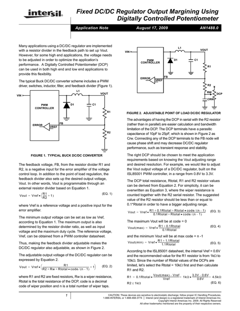
The typical Buck DC/DC converter scheme includes a PWM
driver, switches, inductor, filter, and feedback divider (Figure 1).
August 17, 2009
AN1488.0
L1
VOUT
VIN
D1
PWM
CONTROLLER
C1
R1
ERROR
FB
VREF
R2
L1
RW
VOUT
VIN
DCP
CRW
D1
PWM
CONTROLLER
ERROR
C1
R1
FIGURE 2. ADJUSTABLE POINT OF LOAD DC/DC REGULATOR
R2
The advantages of having the DCP in serial with the R2 resistor
(rather than in parallel) are easier calculation and bandwidth
limitation of the DCP. The DCP terminals have a parasitic
capacitance of 10pF to 25pF, which is shown in Figure 2 as
Crw. Connecting any of the DCP terminals to the FB node will
cause phase shift and may decrease DC/DC regulator
performance, such as transient response and stability.
FB
VREF
FIGURE 1. TYPICAL BUCK DC/DC CONVERTER
The feedback voltage, FB, from the resistor divider R1 and
R2, is a negative input for the error amplifier of the voltage
control loop. In addition to the point of load regulation, the
feedback divider also sets up the desired output voltage,
Vout. In other words, Vout is programmable through an
external resistor divider based on Equation 1.
R1
Vout = Vref • ⎛ -------- + 1 )
⎝ R2
(EQ. 1)
where Vref is a reference voltage and a positive input for the
error amplifier.
The minimum output voltage can be set as low as Vref,
according to Equation 1. The maximum output is also
determined by the resistor divider ratio, as well as input
voltage and the maximum duty cycle. The reference voltage,
Vref, can be obtained from a PWM controller datasheet.
Thus, making the feedback divider adjustable makes the
DC/DC regulator also adjustable, as shown in Figure 2.
The adjustable output voltage of the DC/DC regulator can be
expressed by Equation 2.
R1
Vout = Vref • ⎛ ----------------------------------------------------------------------------------------- + 1⎞
⎝ R2 + Rw + Rtotal • code ⁄ ( n – 1 )
⎠
(EQ. 2)
where R1 and R2 are fixed resistors, Rw is a wiper resistance,
Rtotal is the total resistance of the DCP, code is a decimal
code of wiper position and n is a total number of wiper taps.
1
The right DCP should be chosen to meet the application
requirements based on knowing the Vout adjusting range
and desired resolution. For example, we would like to adjust
the Vout output voltage of a DC/DC regulator, built on the
ISL85001 PWM controller, in a range from 0.8V to 3.3V.
The DCP total resistance, Rtotal, R1 and R2 resistor values
can be derived from Equation 2. For simplicity, it can be
overwritten as Equation 3, where the wiper resistance is
counted together with the R2 serial resistor. The suggested
value of the R2 resistor should be less than or equal to
0.1*Rtotal in order to have a bigger adjusting range.
R1 + 0.1Rtotal + Rtotal • code ⁄ ( n – 1 )
Vout = Vref • ----------------------------------------------------------------------------------------------------------0.1Rtotal + Rtotal • code ⁄ ( n – 1 )
(EQ. 3)
The maximum Vout will be at code = 0
R1 + 0.1Rtotal
Vout ( max ) = Vref • ----------------------------------------0.1Rtotal
(EQ. 4)
and the minimum Vout will be at max code = n -1
R1 + 1.1Rtotal
Vout ( min ) = Vref • ----------------------------------------1.1Rtotal
(EQ. 5)
According to the ISL85001 datasheet, the internal Vref = 0.6V
and the recommended value for the R1 resistor is from 1kΩ to
10kΩ. Since the number of Rtotal values of the DCPs are
limited, let’s select the Rtotal = 10kΩ first and then calculate
R1 and R2.
Vout ( max ) – Vref
3.3V – 0.6V
R1 = 0.1Rtotal • ------------------------------------------------- = 1kΩ • ------------------------------- = 4.5kΩ
Vref
0.6V
(EQ. 6)
R2 ≤ 1kΩ
CAUTION: These devices are sensitive to electrostatic discharge; follow proper IC Handling Procedures.
1-888-INTERSIL or 1-888-468-3774 | Intersil (and design) is a registered trademark of Intersil Americas Inc.
Copyright Intersil Americas Inc. 2009. All Rights Reserved
All other trademarks mentioned are the property of their respective owners.
Application Note 1488
Thus, the ideal DCP for this example should have an Rtotal
resistance of 10kΩ and minimum wiper resistance.
4.0
3.5
3.0
VOUT (V)
There are some other features that should be taken into
account when choosing the appropriate DCP, such as digital
interface, non-volatile programmability, Rtotal tolerance and
Temperature Coefficient (TCr). Most of the available DCPs
on the market have a ±20% Rtotal tolerance from part to
part. That means each DC/DC regulator requires calibration
and that the calibrated value of the wiper position can be
stored in the non-volatile memory.
The perfect solution for DC/DC margining uses a 1%
precision DCP, like the ISL22317, which eliminates the
necessity of individual calibration and provides 0Ω of wiper
resistance and low TCr. The Vout curve versus ISL22317W
tap position is shown in Figure 3. Since Equation 2 is a
hyperbola, the Vout resolution per step changes with the tap
position, from 50mV per tap at the low end to 2mV per tap at
the high end of the DCP settings in our example.
2.5
2.0
1.5
1.0
0.5
0.0
0
20
40
60
80
100
TAP POSITION (DECIMAL)
120
FIGURE 3. THE ISL85001 VOUT vs THE ISL22317W TAP
POSITION
Intersil Corporation reserves the right to make changes in circuit design, software and/or specifications at any time without notice. Accordingly, the reader is cautioned to
verify that the Application Note or Technical Brief is current before proceeding.
For information regarding Intersil Corporation and its products, see www.intersil.com
2
AN1488.0
August 17, 2009
