Introduction to Field Programmable Gate Array (FPGA)
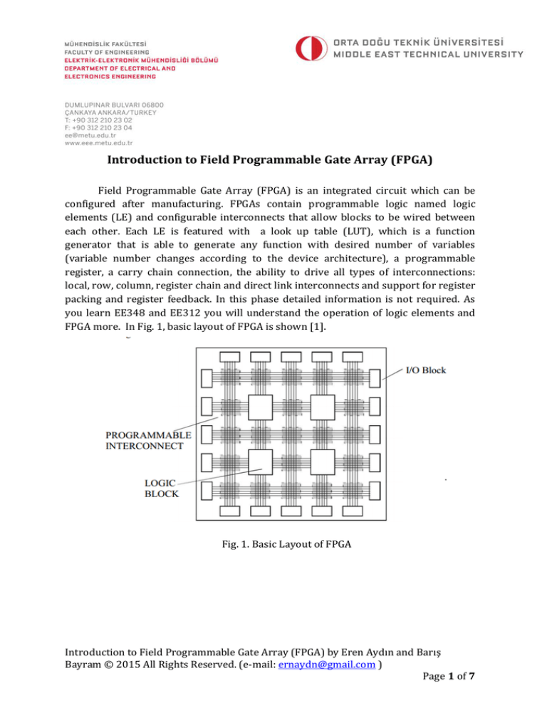
Field Programmable Gate Array (FPGA) is an integrated circuit which can be
configured after manufacturing. FPGAs contain programmable logic named logic
elements (LE) and configurable interconnects that allow blocks to be wired between
each other. Each LE is featured with a look up table (LUT), which is a function
generator that is able to generate any function with desired number of variables
(variable number changes according to the device architecture), a programmable
register, a carry chain connection, the ability to drive all types of interconnections:
local, row, column, register chain and direct link interconnects and support for register
packing and register feedback. In this phase detailed information is not required. As
you learn EE348 and EE312 you will understand the operation of logic elements and
FPGA more. In Fig. 1, basic layout of FPGA is shown [1].
Fig. 1. Basic Layout of FPGA
Introduction to Field Programmable Gate Array (FPGA) by Eren Aydın and Barış
Bayram © 2015 All Rights Reserved. (e-mail: ernaydn@gmail.com )
Page 1 of 7
Logic circuits are designed using different methods which are gate level design,
RTL design and behavioral design.
Gate Level Design: In this method, the desired circuit is designed interconnecting
basic logic gates each other. It is useful for small or medium sized circuit designs but as
the size of the desired circuit increases, gate level design becomes more complicated
and useless.
RTL (Register Transfer Level) Design: In this method, hardware is described
implying logic, defining Flip Flops, latches and how data is transferred between them.
In this method the circuit is implemented using Hardware Description Languages
(HDLs) such as Verilog or HDL. The implemented code is converted into gate level by
logic synthesizers.
Behavioral Design: Overall behavior of the circuit is defined. This method usually is
not synthesizable.
Typical FPGA Design Flow
In Fig. 2, typical design flow of FPGA is given [2].
Fig. 2: Basic FPGA Design Flow
EE 314 Digital Electronics Laboratory
Page 2 of 7
Design Entry: The desired circuit is designed with schematic design or using a
hardware description language.
Synthesis: The designed circuit is synthesized into a circuit consisting of logic
elements provided in the FPGA chip.
Functional Simulation: The synthesized circuit is tested for verification of function of
the designed circuit. Timing issues (propogation delay) are not considered in this
phase.
Fitting: The CAD Fitter tools determine the placement of LEs in an actual FPGA chip. It
also chooses routing wires in the chip to make required connections between LEs.
Timing Analysis: A Propagation delay along the various paths in the fitted circuit is
analyzed to have estimation about the real performance of the designed circuit.
Timing Simulation: This simulation is done to understand both function and timing
performance of the designed circuit.
Programming and Configuration: The designed circuit is implemented in FPGA chip
programming the configuration that configure LEs and establish the required wiring
connections.
EE 314 Digital Electronics Laboratory
Page 3 of 7
DE1-SoC Board
In EE314, you are going to use Altera’s DE1-SoC development board.
Specifications of the board and hardware on the board are written below:
FPGA Device
•
•
•
•
•
•
Cyclone V SoC 5CSEMA5F31C6 Device
Dual-core ARM Cortex-A9 (HPS)
85K Programmable Logic Elements
4,450 Kbits embedded memory
6 Fractional PLLs
2 Hard Memory Controllers
Configuration and Debug
•
•
Serial Configuration device – EPCS128 on FPGA
On-Board USB Blaster II (Normal type B USB connector)
Memory Device
•
•
•
64MB (32Mx16) SDRAM on FPGA
1GB (2x256Mx16) DDR3 SDRAM on HPS
Micro SD Card Socket on HPS
Communication
•
•
•
•
•
Two Port USB 2.0 Host (ULPI interface with USB type A connector)
USB to UART (micro USB type B connector)
10/100/1000 Ethernet
PS/2 mouse/keyboard
IR Emitter/Receiver
Connectors
•
•
•
Two 40-pin Expansion Headers (voltage levels: 3.3V)
One 10-pin ADC Input Header
One LTC connector (One Serial Peripheral Interface (SPI) Master ,one I2C and
one GPIO interface )
EE 314 Digital Electronics Laboratory
Page 4 of 7
Display
•
Audio
•
24-bit VGA DAC
24-bit CODEC, Line-in, line-out, and microphone-in jacks
Video Input
•
ADC
•
•
•
•
TV Decoder (NTSC/PAL/SECAM) and TV-in connector
Fast throughput rate: 1 MSPS
Channel number: 8
Resolution: 12 bits
Analog input range : 0 ~ 2.5 V or 0 ~ 5V as selected via the RANGE bit in the
control register
Switches, Buttons and Indicators
•
•
•
•
•
4 User Keys (FPGA x4)
10 User switches (FPGA x10)
11 User LEDs (FPGA x10 ; HPS x 1)
2 HPS Reset Buttons (HPS_RST_n and HPS_WARM_RST_n)
Six 7-segment displays
Sensors
•
Power
•
G-Sensor on HPS
12V DC input
EE 314 Digital Electronics Laboratory
Page 5 of 7
Block Diagram of the DE1-SOC Board
DE1_SoC Board Specifications
EE 314 Digital Electronics Laboratory
Page 6 of 7
Top View of the Board
REFERENCES
[1] EXPERIMENT NUMBER 3 INTRODUCTION TO FIELD PROGRAMMABLE GATE ARRAYS AND LOGIC,
http://ece.mst.edu/media/academic/ece/documents/classexp/cpe112/cpe112labs/CpE_112_LAB_3.pdf
[2] Quartus II Introduction to Schematics Tutorial
EE 314 Digital Electronics Laboratory
Page 7 of 7


