International Journal of Innovative Research in Advanced Engineering (IJIRAE)
Volume 1 Issue 9 (October 2014)
ISSN: 2349-2163
www.ijirae.com
Simulation of single phase SPWM (Unipolar) inverter
SACHIN MAHESHRI
PRABODH KHAMPARIYA
Electrical Engg.Dept.
S. S. S. I.T & M.S., Sehore M.P.
Electrical Engg.Dept.
S. S. S. I.T & M.S., Sehore M.P.
Abstract- In this paper, a simulation of SPWM (Unipolar) strategy is presented for single phase full bridge inverter. The
simulation of the single-phase unipolar voltage switching inverter device model is simulated in Matlab/Simulink. The
modulation ratio change from 0.4 to 0.9 by varying amplitude of modulating signal. The outputs voltage and current %THD
waveforms for variable AC voltages and modulation index are observed on scope, and also see the THD.SPWM techniques are
characterized by constant amplitude pulses with different duty cycle for each period. The width of this pulses are modulated in
order to obtain inverter output voltage control and to reduce its harmonic content. Sinusoidal pulse width modulation or
SPWM is the most common method in motor control and inverter application. Conventionally, to generate the signal, triangle
wave as a carrier signal is compared with the sinusoidal wave, whose frequency is the desired frequency. In next the hardware
design for unipolar voltage switching for inverter for fixed modulation index and is tested for different resistive loads.
Keywords-Sinusoidal pulse width modulation (SPWM), Bipolar, Total Harmonic distortion (THD). Pulse Width Modulation
(PWM), UPS (uninterruptible power supplies).
I. INTRODUCTION
An inverter is basically a device that converts electrical energy of DC form into that of AC. The purpose of DC-AC
inverter is to take DC power from a battery source and converts it to AC. The inverter receives DC supply from 12V battery and
then inverter converts it to 230V AC with a desirable frequency of 50Hz. These DC-AC inverters have been widely used for
industrial applications such as uninterruptible power supply (UPS), AC motor drives. In addition to this, the control strategies
used in the inverters are also similar to those in DC-DC converters. Both current-mode control and voltage-mode control are
employed in practical applications.
A voltage source inverter employing thyristor as switches, some type of forced commutation is required, while the VSI
made up of using GTOs, power transistors, power MOSFETs or IGBTs. A standard single-phase voltage or current source
inverter can be in the half-bridge or full-bridge configuration. Some industrial applications of inverters are for adjustable-speed ac
drives, UPS (uninterruptible power supplies) for computers, HVDC transmission lines, induction heating, standby aircraft power
supplies etc.
II. PULSE WIDTH MODULATION (PWM) TECHNIQUE IN INVERTER
The Modulation Process is Included in Inverter for Switching. A basic of Pulse Width Modulation (PWM) Technique is
as. There are many forms of modulation used for communicating information. When a high Frequency signal has amplitude
varied in response to a lower frequency signal we have AM (amplitude modulation).When the signal frequency is varied in
response to the modulating signal we have FM (frequency modulation. These signals are used for radio modulation because the
high frequency carrier signal is needs for efficient radiation of the signal. When communication by pulses was introduced, the
amplitude, frequency and pulse width become possible modulation options. In many power electronic converters where the output
voltage can be one of two values, the only option is modulation of average conduction time.
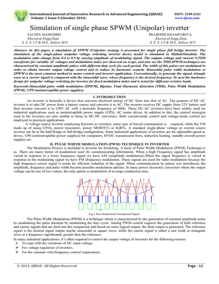
Fig.1 Sine Modulated,Unmodulated Signal
The Pulse Width Modulation (PWM) is a technique which is characterized by the generation of constant amplitude pulse
by modulating the pulse duration by modulating the duty cycle. Analog PWM control requires the generation of both reference
and carrier signals that are feed into the comparator and based on some logical output, the final output is generated. The reference
signal is the desired signal output maybe sinusoidal or square wave, while the carrier signal is either a saw tooth or triangular
wave at a frequency significantly greater than the reference.
In many industrial applications, it’s often required to control the output voltage of inverters for the following reasons
To cope with the variations of DC input voltage.
For voltage regulation of inverters.
For the constant volts/frequency control requirement.
________________________________________________________________________________________________________
© 2014, IJIRAE- All Rights Reserved
Page - 12
International Journal of Innovative Research in Advanced Engineering (IJIRAE)
Volume 1 Issue 9 (October 2014)
ISSN: 2349-2163
www.ijirae.com
There are various techniques to vary the inverter gain. The most efficient method of controlling the gain (and output
voltage) is to integrate pulse width modulation (PWM) control within the inverters. The commonly used techniques are. There
are five basic PWM techniques:
1. Linear modulation
2. Saw tooth PWM
3. Single Pulse Width Modulation
4. Multiple Pulse Width Modulation
5. Sinusoidal Pulse Width Modulation
III. SINUSOIDAL PULSE WIDTH MODULATION (SPWM)
Instead of, maintaining the width of all pulses of same as in case of multiple pulse width modulation, the width of each pulse
is varied in proportion to the amplitude of a sine wave evaluated at the centre of the same pulse. The distortion factor and lower
order harmonics are reduced significantly. The gating signals are generated by comparing a sinusoidal reference signal with a
triangular carrier wave of frequency Fc.The frequency of reference signal Fr ,determines the inverter output frequency and its
peak amplitude Ar,controls the modulation index M,and Vrms output voltage VO.The number of pulses per half cycle depends
on carrier frequency .
Inverters that use PWM switching techniques have a DC input voltage that is usually constant in magnitude. The inverters
job is to take this input voltage and output ac where the magnitude and frequency can be controlled. There are many different
ways that pulse-width modulation can be implemented to shape the output to be AC power. A common technique called
sinusoidal-PWM will be explained. In order to output a sinusoidal waveform at a specific frequency a sinusoidal control signal at
the specific frequency is compared with a triangular waveform. The inverter then uses the frequency of the triangle wave as the
switching frequency. This is usually kept constant.
The triangle waveform, vtri, is at switching frequency fs; this frequency controls the speed at which the inverter switches are
turned off and on. The control signal, vcontrol, is used to modulate the switch duty ratio and has a frequency f1. This is the
fundamental frequency of the inverter voltage output. Since the output of the inverter is affected by the switching frequency it
will contain harmonics at the switching frequency. The duty cycle of the one of the inverter switches is called the amplitude
modulation ratio, ma.
Fig.2 Desired Frequency is compared with a Triangular Waveform.
Fig.3 Pulse-width Modulation (PWM)
Vcontrol<Vtri
TA- : on, TA+: off
TA+: on, TA- : off
m a
Vcontrol>Vtri
VAo, fundamental= (VAO)
V control
V tri
Where V control is the peak amplitude of the control signal
v control
v tri
Ta_pos is on,
vA
Vd
2
V
m
f s
f
f 1
d
Ta_neg is on,
v control
v tri
vA
The
switches Ta+ and Ta- are controlled based on the comparison of
2
________________________________________________________________________________________________________
© 2014, IJIRAE- All Rights Reserved
Page - 13
International Journal of Innovative Research in Advanced Engineering (IJIRAE)
Volume 1 Issue 9 (October 2014)
ISSN: 2349-2163
www.ijirae.com
Vcontrol and Vtri .The two switches are never off at the same time which results in the output voltage fluctuating between +/- Vd/2.
In order to fulfill the requirement, the new switching technique had been analyzed and recommended in this paper,
namely SPWM which is generated by PIC microcontroller. The various frequency triangular carriers with different amplitude
modulation ratio SPWM signal had been programmed and tested in single phase inverter circuit in order to find the best switching
signal in simulink.
Switching Losses.
Utilization of DC power supply that is to deliver a higher output voltage with the same DC supply.
Linearity in voltage and current control.
Harmonics contents in the voltage and current.
IV.PWM Switching Techniques
The PWM switching can be divided into two switching scheme which are PWM with Bipolar voltage switching and
PWM with Unipolar voltage switching
1. PWM with Bipolar voltage switching
2. PWM with Unipolar voltage switching
Power inverter converts DC power to AC.There are several methods to do this. The two main ways, which use switched
mode inverters, are square wave and pulse width modulation. The DC input voltage is adjusted to control the AC output
magnitude of a square wave inverter. The switching frequency is adjusted to control the frequency. However, the methods used
for a square wave inverter differ for a pulse width modulated inverter. In PWM, the controller adjusts both the magnitude and
frequency. The difference in switching causes the harmonics to appear at different locations. Although the square wave signals
are simpler, the harmonics exist mostly in the lower frequencies, which are close to the output frequency. In a PWM inverter, the
harmonics are at multiples of the fundamental frequency, and thus are easier to filter. As a result, the output sinusoid has less
distortion. Unfortunately, a PWM hold a major disadvantage in requiring complex switching circuitry as well as increased
switching loss.
V. PWM with Unipolar Voltage Switching
The two types of pulse width modulation inverters are bipolar and unipolar switching. Each unique switching technique creates
either a unipolar or bipolar output at the load. The control signals depend on comparing a reference signal and carrier signal. A
PWM requires a sinusoidal reference signal and triangular carrier signal.
Fig.4 Full Bridge Inverter.
Fig.5 Unipolar PWM generators
There are two types of unipolar switching. Type one operates both switches pairs at a high frequency. Type two uses a
high frequency for one pair and a low frequency for the other pair of switches. We will be building a type two unipolar PWM
inverter because it is simpler than type one. Fig.6 shows the output voltage switching characteristics for type two unipolar
switching. The switching conditions are shown in Fig.6 (a) where Vsine and Vtri are the sine wave and triangular wave control
signals respectively.
Fig.6 Waveform for SPWM with Unipolar voltage switching
________________________________________________________________________________________________________
© 2014, IJIRAE- All Rights Reserved
Page - 14
International Journal of Innovative Research in Advanced Engineering (IJIRAE)
Volume 1 Issue 9 (October 2014)
ISSN: 2349-2163
www.ijirae.com
In this scheme, the triangular carrier waveform is compared with two reference signals, which are positive and negative
signal. The basic idea to produce SPWM with unipolar voltage switching is shown in Fig.6 (a). The difference between the
Bipolar SPWM generators is that the generator uses another comparator to compare between the inverse reference waveform−Vr .
The process of comparing these two signals to produce the unipolar voltage-switching signal. In Unipolar voltage switching the
output voltage switches between 0 and Vdc, or switching event is halved in the Unipolar case from 2Vdc to Vdc. The effective
switching frequency is seen by the load is doubled and the voltage pulse amplitude is halved. Due to this, the harmonic content of
the output voltage waveform is reduced compared to bipolar switching. In Unipolar voltage switching scheme also, the amplitude
of the significant harmonics and its sidebands is much lower for all modulation indexes thus making filtering easier, and with its
size being significantly smaller. Between 0 and −Vdc. This is in contrast to the bipolar switching strategy in which the output
swings between Vdc and −Vdc. As a result, the change in output voltage at each.
(a) Comparison between reference waveform and triangular waveform
(b) Gating pulses for S11 and S22
(c) Gating pulses for S12 and S21
(d) Output waveform.
In this scheme, the devices in one leg are turned on or off based on the comparison of the modulation signal Vr with a
high frequency triangular wave. The devices in the other leg are turned on or off by the comparison of the modulation signal – Vr
with the same high frequency triangular wave.
The logic behind the switching of the devices in the leg connected to ‘a’ is given as,
Vr > Vc S11 is on === > Van = Vd and
2
Vr<Vc S12 is on===> Van = - Vd
2
and that in the leg connected to ‘b’ is given as
- Vr > Vc S11 is on === > Vbn = Vd
2
-Vr>Vc S11 is on == > Vbn = - Vd
2
In Unipolar switching scheme the output voltage level changes between either 0 to –Vd or from 0 to +Vd. This scheme
‘effectively’ has the effect of doubling the switching frequency as far as the output harmonics are concerned, compared to the
bipolar- switching scheme.
VI. SOFTWARE SYSTEM DEVELOPMENT USING MATLAB
In looking at the components selected and the simulations created before the actual construction of the inverter,
everything was built in mind for the purpose of efficiency and keeping power losses to a minimum. Nowadays in so many
applications desire controlled A.C. for controlling speed of machines like Induction Motor, Brushless D.C. Motor etc. For getting
controlled A.C. nowadays inverter is used. Inverter is converting uncontrolled D.C. in to controlled A.C. There are so many types
of inverter like two level, three level and five level etc. This is a very simple technique for harmonic reduction. In this technique
pulse magnitude will be constant and only pulse time (width) can be changed. In this pure sine wave is compared with carrier
(triangular) wave and producing gate pulses. Sine wave has fundamental frequency and carrier wave can be taken more than
fundamental frequency. This is a very simple technique for harmonic reduction. In this technique pulse magnitude will be
constant and only pulse time (width) can be changed. In this pure sine wave is compared with carrier (triangular) wave and
producing gate pulses. Sine wave has fundamental frequency and carrier wave can be taken more than fundamental frequency. In
this simulation development of two level inverter has discussed and output voltage and current waveforms, and its harmonics
reduction by varing the modulation index.
VII. BLOCK DIAGRAM OF THE SPWM SYSTEM
Fig. 7 Block Diagram of the SPWM Inverter
________________________________________________________________________________________________________
© 2014, IJIRAE- All Rights Reserved
Page - 15
International Journal of Innovative Research in Advanced Engineering (IJIRAE)
Volume 1 Issue 9 (October 2014)
a)
b)
c)
d)
ISSN: 2349-2163
www.ijirae.com
Ideal DC Voltage Source
The DC Voltage Source block implements an ideal DC voltage source. The positive terminal is represented by a
plus sign on one port. You can modify the voltage at any time during the simulation.
MOSFET Inverter Bridge Section
It consists of two or Four semiconductor switches, according to Configuration either half or full bridge.Here we
use four MOSFET’s which are connected to form a full bridge circuit. The input to the bridge is the output of the filtered
rectified DC voltage. The gates of the MOSFET s are triggered using the PWM pulses.
Discrete PWM Generator
This Discrete block generates pulses for Carrier-based PWM (Pulse Width Modulation).depending on the
number of arms in the selected mode parameter, the blocks can be used either for single-phase or three-phase PWM
Control.
Filter and Load Circuit
The last block is filter and load circuit. The branch resistance, in ohms (Ω (100Ohm) acts as a load. In next the
outputs from the MOSFET’s have some harmonics. The harmonics can be filtered using filter circuit.
VIII. SIMULINK MODEL OF UNIPOLAR AND BIPOLAR VOLTAGE SWITCHING
Fig.8 Single Phase Inverter MATLAB Simulink Model
The Simulation diagram for single phase inverter drawn using MATLAB SIMULINK is shown in Fig.8, the simulation model
diagram consists of the following blocks.
DC Supply (Vdc2)
MOSFET bridge Section(s1,s2,s3,s4)
PWM Pulse Generator
Filter and Load Circuit
MOSFET INVERTER BRIDGE SECTION
The metal-oxide semiconductor field-effect transistor (MOSFET) is a semiconductor device controllable by the gate
signal (g > 0). The MOSFET device is connected in parallel with an internal diode that turns on when the MOSFET device is
reverse biased (Vds < 0) and no gate signal is applied (g=0). The model is simulated by an ideal switch controlled by a logical
signal (g > 0 or g = 0), with a diode connected in Parallel .here we use four MOSFET’s which are connected to form a bridge
circuit. The input to the bridge is the output of the filtered rectified DC voltage. The gates of the MOSFET s are triggered using
the PWM pulses. The parameters are given below.
IX. PWM PULSE GENERATOR FOR UNIPOLAR VOLTAGE SWITCHING
The output pulses are a vector (with values=0 or 1). Depending on the selected "Generator Mode", the output vector
contains: For a 1-arm bridge: Two pulses. Pulse 1 is for the upper switch and pulse 2 is for the lower switch. For a 2-Arm Bridge:
Four pulses. Pulses 1 and 3 are respectively for the upper switches of the first and second arm. Pulses 2 and 4 are for the lower
switches. For a 3-arm bridge: Six pulses. Pulses 1,3 and 5 are respectively for the upper switches of the first, second and third
arm. Pulses 2, 4 and 6 are for the lower switches. For double 3-arm bridges: Twelve pulses. The first six pulses (pulses 1 to 6)
must be sent to the first 3-arm bridge and the last six (pulses 7 to 12) to the second 3-arm bridge.
By selecting "Internal generation" you can control the modulation index m, frequency and phase of the output voltage from the
________________________________________________________________________________________________________
© 2014, IJIRAE- All Rights Reserved
Page - 16
International Journal of Innovative Research in Advanced Engineering (IJIRAE)
Volume 1 Issue 9 (October 2014)
ISSN: 2349-2163
www.ijirae.com
internal parameters (m, Freq.and Phase). Otherwise, external signals are used for pulse generation. The width of the input vector
must be 1 for single phase bridges (1-arm or 2-arm) and 3 for 3-phase bridges (single or double bridge).
Fig.9 SPWM Pulse Generator Circuit
Figure 9 shows SPWM Pulse Generator Circuit in that we use two sine wave signal (reference signal) has phase opposite
to each other. It is compared with triangular wave (switching signal).in comparator gives switching pulses to the MOSFETs.
X. GATE PULSES GENERATION FOR UNIPOLAR VOLTAGE SWITCHING
SineWave (Reference w ave)
10
0
-10
0
10
5
0
0
1
0.5
0
0
1
0.5
0
0
1
0.5
0
0
1
0.5
0
0
a
0.01
0.02
0.03
0.04
0.05
T riangular Wav e)
0.06
0.07
0.08
0.09
0.1
b
0.01
0.02
0.03
0.04
0.05
0.06
0.07
0.08
0.09
0.1
0.01
0.02
0.03
0.04
0.05
0.06
0.07
0.08
0.09
0.1
c
d
0.01
0.02
0.03
0.04
0.05
0.06
0.07
0.08
0.09
0.1
0.01
0.02
0.03
0.04
0.05
0.06
0.07
0.08
0.09
0.1
0.01
0.02
0.03
0.04
0.05
0.06
0.07
0.08
0.09
0.1
e
f
T ime
Fig.10 Waveforms for SPWM with Unipolar voltage switching (a) Reference waveforms (b) Triangular waveform,(c),(d),(e),(f)gating pulses for S11 ,S12 ,S21
and S22.resp.after sine and triangular wave comparison
XI. GATE PULSES WAVEFORMS
The PWM pulse generator block generator block generator block generates the four PWM pulses and these pulses are given to the
gates of the MOSFET s for turning on and turn off.
Fig. 11 Gating Pulses for S11, S12, S22 and S21
XII. RESULT Simulation Waveform
current (I load)
0.2
0.1
0
-0.1
-0.2
0
0.01
0.02
0.03
0.04
0.05
0.06
0.07
0.08
0.09
0.1
0.07
0.08
0.09
0.1
voltage (V load)
10
0
-10
0
0.01
0.02
0.03
0.04
0.05
Time
0.06
Fig. 12 Output voltage and current waveform of Unipolar Voltage Switching without filter
________________________________________________________________________________________________________
© 2014, IJIRAE- All Rights Reserved
Page - 17
International Journal of Innovative Research in Advanced Engineering (IJIRAE)
Volume 1 Issue 9 (October 2014)
ISSN: 2349-2163
www.ijirae.com
current
0.1
0
-0.1
0
0.01
0.02
0.03
0.04
0.05
0.06
0.07
0.08
0.09
0.1
0.06
0.07
0.08
0.09
0.1
voltage
10
0
-10
0
0.01
0.02
0.03
0.04
0.05
Time
Fig.13 Output voltage and current waveform of Unipolar Voltage Switching with filter
XIII. CONCLUSION
The electronic devices is smaller, therefore the efficiency of power supply used in electronic devices should be improved
from time to time. The different switching techniques and switching elements were used in single phase inverter also considered
when inverters become the best power supply for converting DC power to AC power. Based on studied, SPWM techniques is a
common method used in single phase inverter circuit are Unipolar and Bipolar voltage Switching. The simulation of the singlephase Unipolar voltage switching inverter device model is simulated in Matlab/Simulink.
XIV. REFERENCES
[1]
[2]
[3]
[4]
[5]
[6]
[7]
[8]
[9]
[10]
[11]
[12]
[13]
Pankaj H Zope, Pravin G.Bhangale, Prashant Sonare ,S. R.Suralkar “Design and Implementation of carrier based
Sinusoidal PWM Inverter”, International Journal of Advanced Research in Electrical, Electronics and Instrumentation Engineering,
Vol. 1, Issue 4, October 2012 ISSN: 2278 - 8875
Anand. D & Jeevananthan .S "Modeling and Analysis of Conducted EMI Emissions of a Single-Phase PWM Inverters" Asian Power
Electronics Journal, Vol. 4, No.3 December 2010.
B.Geetalaxmi and P.Dananjayan, “ A Multipulse –Multilevel Inverter Suitable for High Power Application”, International Journal of
Computer and Electrical Engineering,Vol.2 No.2.April,2021 pp-257-261.
J. Kim, J. Hong, K. Nam “ A Current Distortion Compensation Scheme For Four-switch Inverters”, IEEE Transactions on Power
Electronics, Vol. 24, No. 4, April 2009, pp. 1032 – 1040.
Mr. R.Senthilkumar, Prof. M.Singaaravelu “DESIGN OF SINGLE PHASE INVERTER U SING dsPIC30F4013,
International Journal of Engineering Science and Technology Vol. 2(11), 2010, pp.6500-6506. Pardasani Hitendra K, Arora Kapildev
N, “Simulation Of Three Level Inverter Using Sinusoidal Pulse Width Modulation Technique By MATLAB”. National Conference on
Recent Trends in Engineering & Technology, B.V.M. Engineering College, V.V.Nagar,Gujarat,India, 13-14 May 2011.
Mahesh A. Patel, Ankit R. Patel, Dhaval R.Vyas and Ketul M. Patel, “Use of PWM Techniques for Power Quality Improvement”,
International Journal of Recent Trends in Engineering, Vol. 1, No. 4, May 2009.pp.99-102.
C. R. Balamurugan, S. P. Natarajan, V. Padmathilagam, “Comparative Study on Unipolar PWM Strategies for Three Phase Five Level
Cascaded Inverter” European Journal of Scientific Research ISSN 1450-216X Vol.80 No.4 (2012), pp.517-539.
Khanniche, M.S., “A novel switching strategy of a single phase micro controlled UPS system ”, Electrotechnical Conference, 1991.
Proceedings. 6th Mediterranean Publication Year: 1991, vol.2 pp. 1360 – 1362.
Suvarun Dalapati,chandan chakraborty, “A Direct pwm technique for a single phase full bridge inverter through controlled capacitor
caharging”, IEEE transactions on industry applications, vol. 55, no. 8, August 2008 pp.2912-2922.
Nalin Kant Mohanty, Ranganath “Microcontroller Based PWM Controlled Four Switch Three Phase Inverter Fed Induction Motor
Drive” SERBIAN JOURNAL OF ELECTRICAL ENGINEERING Vol. 7, No. 2, November 2010, pp.195-204.
J. S. Lai and F. Z. Feng, “Multilevel converters-a new breed of power converters,” IEEE transaction on industrial applications, Vol.
IA-32, 1996, pp. 509-517.
A. Nabae, I. Takahashi and H. Akagi, "A neutral-point clamped PWM inverter," IEEE transaction on industrial applications, Vol. IA17, 1981, pp. 518-523.
________________________________________________________________________________________________________
© 2014, IJIRAE- All Rights Reserved
Page - 18
