CLA20EF1200PZ
tentative
High Efficiency Thyristor
VDRM
=
1200 V
I TAV
=
20 A
VT
=
1,4 V
Triode
Single Reverse Conducting Thyristor
Part number
CLA20EF1200PZ
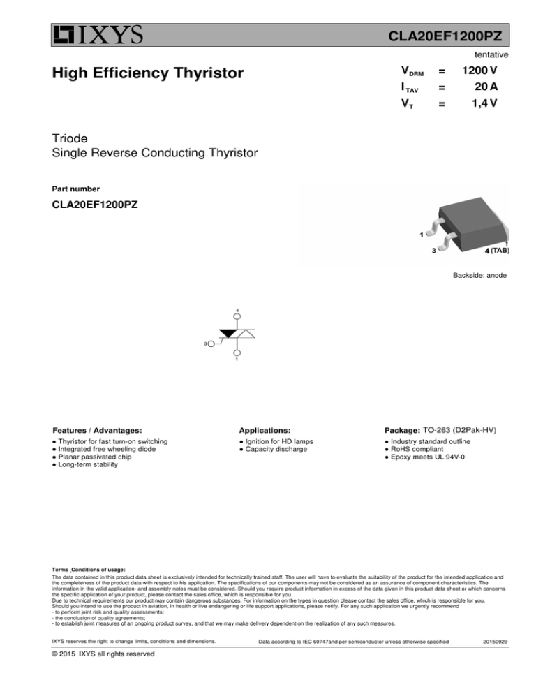
Backside: anode
4
3
1
Features / Advantages:
Applications:
Package: TO-263 (D2Pak-HV)
● Thyristor for fast turn-on switching
● Integrated free wheeling diode
● Planar passivated chip
● Long-term stability
● Ignition for HD lamps
● Capacity discharge
● Industry standard outline
● RoHS compliant
● Epoxy meets UL 94V-0
Terms Conditions of usage:
The data contained in this product data sheet is exclusively intended for technically trained staff. The user will have to evaluate the suitability of the product for the intended application and
the completeness of the product data with respect to his application. The specifications of our components may not be considered as an assurance of component characteristics. The
information in the valid application- and assembly notes must be considered. Should you require product information in excess of the data given in this product data sheet or which concerns
the specific application of your product, please contact the sales office, which is responsible for you.
Due to technical requirements our product may contain dangerous substances. For information on the types in question please contact the sales office, which is responsible for you.
Should you intend to use the product in aviation, in health or live endangering or life support applications, please notify. For any such application we urgently recommend
- to perform joint risk and quality assessments;
- the conclusion of quality agreements;
- to establish joint measures of an ongoing product survey, and that we may make delivery dependent on the realization of any such measures.
IXYS reserves the right to change limits, conditions and dimensions.
© 2015 IXYS all rights reserved
Data according to IEC 60747and per semiconductor unless otherwise specified
20150929
CLA20EF1200PZ
tentative
Ratings
Thyristor
Conditions
Symbol
VDSM
Definition
max. non-repetitive forward blocking voltage
TVJ = 25°C
VDRM
max. repetitive forward blocking voltage
TVJ = 25°C
1200
ID
drain current
TVJ = 25°C
10
µA
1
mA
TVJ = 25°C
1,40
V
1,60
V
1,40
V
IT =
20 A
VF
IF =
40 A
IT =
20 A
IF =
40 A
threshold voltage
rT
slope resistance
R thJC
thermal resistance junction to case
V
TVJ = 125°C
reverse voltage drop
VT0
max. Unit
1300
V
VD = 1200 V
forward voltage drop
average forward current
typ.
VD = 1200 V
VT
I TAV
min.
TVJ = 125 °C
TC = 115 °C
1,60
V
T VJ = 150 °C
20
A
TVJ = 150 °C
0,90
V
25
mΩ
DC
for power loss calculation only
RthCH
thermal resistance case to heatsink
Ptot
total power dissipation
I TSM
max. forward surge current
I²t
value for fusing
0,65 K/W
K/W
0,25
TC = 25°C
190
W
t = 10 ms; (50 Hz), sine
TVJ = 45°C
120
A
t = 8,3 ms; (60 Hz), sine
VR = 0 V
130
A
t = 10 ms; (50 Hz), sine
TVJ = 150 °C
100
A
t = 8,3 ms; (60 Hz), sine
VR = 0 V
110
A
t = 10 ms; (50 Hz), sine
TVJ = 45°C
72
A²s
t = 8,3 ms; (60 Hz), sine
VR = 0 V
70
A²s
t = 10 ms; (50 Hz), sine
TVJ = 150 °C
50
A²s
50
A²s
t = 8,3 ms; (60 Hz), sine
VR = 0 V
CJ
junction capacitance
VR = 400 V f = 1 MHz
TVJ = 25°C
PGM
max. gate power dissipation
t P = 30 µs
T C = 150 °C
6
t P = 300 µs
pF
10
W
5
W
0,5
W
PGAV
average gate power dissipation
(di/dt) cr
critical rate of rise of current
TVJ = 150 °C; f = 50 Hz
repetitive, IT =
t P = 1 µs; di G /dt = 0,5 A/µs; I TSA = 600 A
60 A
500 A/µs
I G = 0,07 A; V = ⅔ VDRM
20 A
1500 A/µs
(dv/dt)cr
critical rate of rise of voltage
V = ⅔ VDRM
VGT
gate trigger voltage
I GT
gate trigger current
VGD
gate non-trigger voltage
I GD
gate non-trigger current
IL
latching current
non-repet., I T =
TVJ = 150°C
500 V/µs
VD = 6 V
TVJ = 25 °C
1,3
TVJ = -40 °C
1,6
V
VD = 6 V
TVJ = 25 °C
20
mA
TVJ = -40 °C
35
mA
TVJ = 150°C
0,2
V
1
mA
TVJ = 25 °C
30
mA
R GK = ∞; method 1 (linear voltage rise)
VD = ⅔ VDRM
tp =
10 µs
IG = 0,07 A; di G /dt =
V
0,5 A/µs
IH
holding current
VD = 6 V R GK = ∞
TVJ = 25 °C
25
mA
t gd
gate controlled delay time
VD = ½ VDRM
TVJ = 25 °C
2
µs
tq
turn-off time
IG = 0,07 A; di G /dt =
VR =
0,5 A/µs
0 V; I T = 20 A; V = ⅔ VDRM TVJ =125 °C
di/dt = 10 A/µs dv/dt =
IXYS reserves the right to change limits, conditions and dimensions.
© 2015 IXYS all rights reserved
150
µs
20 V/µs t p = 200 µs
Data according to IEC 60747and per semiconductor unless otherwise specified
20150929
CLA20EF1200PZ
tentative
Package
Ratings
TO-263 (D2Pak-HV)
Symbol
I RMS
Definition
Conditions
RMS current
per terminal
min.
TVJ
virtual junction temperature
T op
operation temperature
Tstg
storage temperature
-40
max.
35
Unit
A
-40
150
°C
-40
125
°C
150
°C
1,5
Weight
FC
20
mounting force with clip
d Spp/App
typ.
Product Marking
C
L
A
20
EF
1200
PZ
IXYS Zyyww
Logo
Assembly Line
Date Code
N
4,2
mm
terminal to backside
4,7
mm
Part description
XXXXXXXXX
Part No.
60
terminal to terminal
creepage distance on surface | striking distance through air
d Spb/Apb
g
=
=
=
=
=
=
=
Thyristor (SCR)
High Efficiency Thyristor
(up to 1200V)
Current Rating [A]
Single Reverse Conducting Thyristor
Reverse Voltage [V]
TO-263AB (D2Pak) (2HV)
000000
Assembly Code
Ordering
Standard
Ordering Number
CLA20EF1200PZ
Equivalent Circuits for Simulation
I
V0
R0
Marking on Product
CLA20EF1200PZ
* on die level
Delivery Mode
Tape & Reel
Code No.
T VJ = 150 °C
Thyristor
V 0 max
threshold voltage
0,9
V
R0 max
slope resistance *
22
mΩ
IXYS reserves the right to change limits, conditions and dimensions.
© 2015 IXYS all rights reserved
Quantity
800
Data according to IEC 60747and per semiconductor unless otherwise specified
20150929
CLA20EF1200PZ
tentative
Outlines TO-263 (D2Pak-HV)
Dim.
W
Supplier
Option
D1
L1
c2
A1
H
D
E
A
1
4
3
L
e1
D2
A2
c
2x e
2x b2
10.92
(0.430)
2x b
mm (Inches)
W
Inches
min
max
0.160 0.190
typ. 0.004
0.095
0.020 0.039
0.045 0.055
0.016 0.029
0.045 0.055
0.330 0.370
0.315 0.350
0.091
0.380 0.410
0.245 0.335
0,100 BSC
0.169
0.575 0.625
0.070 0.110
0.040 0.066
typ.
0.002
0.0008
All dimensions conform with
and/or within JEDEC standard.
1.78
(0.07)
3.05
(0.120)
3.81
(0.150)
9.02
(0.355)
E1
A
A1
A2
b
b2
c
c2
D
D1
D2
E
E1
e
e1
H
L
L1
Millimeter
min
max
4.06
4.83
typ. 0.10
2.41
0.51
0.99
1.14
1.40
0.40
0.74
1.14
1.40
8.38
9.40
8.00
8.89
2.3
9.65
10.41
6.22
8.50
2,54 BSC
4.28
14.61 15.88
1.78
2.79
1.02
1.68
typ.
0.040
0.02
2.54 (0.100)
Recommended min. foot print
4
3
1
IXYS reserves the right to change limits, conditions and dimensions.
© 2015 IXYS all rights reserved
Data according to IEC 60747and per semiconductor unless otherwise specified
20150929


