A Basic Property of MOS Transistors and its Circuit Implications
advertisement
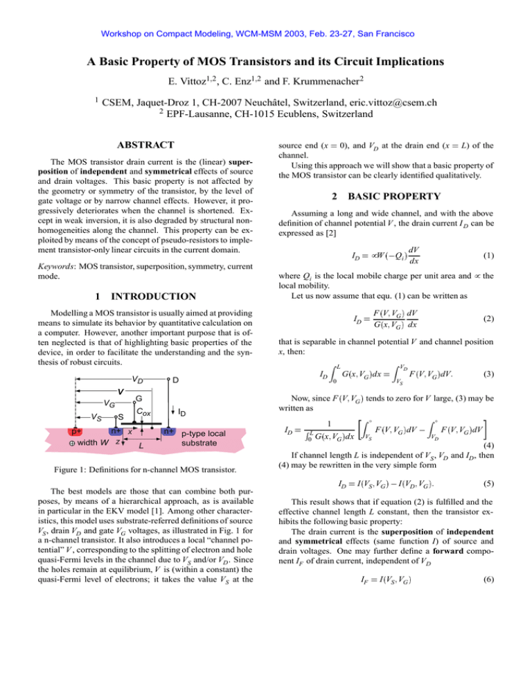
Workshop on Compact Modeling, WCM-MSM 2003, Feb. 23-27, San Francisco A Basic Property of MOS Transistors and its Circuit Implications E. Vittoz1;2 , C. Enz1;2 and F. Krummenacher2 1 CSEM, Jaquet-Droz 1, CH-2007 Neuchâtel, Switzerland, eric.vittoz@csem.ch 2 EPF-Lausanne, CH-1015 Ecublens, Switzerland ABSTRACT The MOS transistor drain current is the (linear) superposition of independent and symmetrical effects of source and drain voltages. This basic property is not affected by the geometry or symmetry of the transistor, by the level of gate voltage or by narrow channel effects. However, it progressively deteriorates when the channel is shortened. Except in weak inversion, it is also degraded by structural nonhomogeneities along the channel. This property can be exploited by means of the concept of pseudo-resistors to implement transistor-only linear circuits in the current domain. Keywords: MOS transistor, superposition, symmetry, current mode. 1 INTRODUCTION Modelling a MOS transistor is usually aimed at providing means to simulate its behavior by quantitative calculation on a computer. However, another important purpose that is often neglected is that of highlighting basic properties of the device, in order to facilitate the understanding and the synthesis of robust circuits. VD V VG VS S n+ x p+ width W z L 2 ID n+ p-type local substrate Figure 1: Definitions for n-channel MOS transistor. The best models are those that can combine both purposes, by means of a hierarchical approach, as is available in particular in the EKV model [1]. Among other characteristics, this model uses substrate-referred definitions of source VS , drain VD and gate VG voltages, as illustrated in Fig. 1 for a n-channel transistor. It also introduces a local “channel potential” V , corresponding to the splitting of electron and hole quasi-Fermi levels in the channel due to VS and/or VD . Since the holes remain at equilibrium, V is (within a constant) the quasi-Fermi level of electrons; it takes the value VS at the BASIC PROPERTY Assuming a long and wide channel, and with the above definition of channel potential V , the drain current I D can be expressed as [2] ID = µW ( Qi ) dV dx (1) where Qi is the local mobile charge per unit area and µ the local mobility. Let us now assume that equ. (1) can be written as F (V; VG ) dV G(x; VG ) dx ID = (2) that is separable in channel potential V and channel position x, then: Z L ID D G Cox source end (x = 0), and VD at the drain end (x = L) of the channel. Using this approach we will show that a basic property of the MOS transistor can be clearly identified qualitatively. 0 G(x; VG )dx = Z V D VS F (V; VG )dV: (3) Now, since F (V; VG ) tends to zero for V large, (3) may be written as ID = R L 0 Z 1 G(x; VG )dx VS Z ∞ ∞ F (V; VG )dV VD F (V; VG )dV (4) If channel length L is independent of VS , VD and ID , then (4) may be rewritten in the very simple form ID = I (VS ; VG ) I (VD ; VG ): (5) This result shows that if equation (2) is fulfilled and the effective channel length L constant, then the transistor exhibits the following basic property: The drain current is the superposition of independent and symmetrical effects (same function I) of source and drain voltages. One may further define a forward component IF of drain current, independent of VD IF = I (VS ; VG ) (6) 4 and a reverse component IR , independent of VS IR = I (VD ; VG ): (7) It is interesting to point out that the above property is similar to that of bipolar transistors as expressed by the EbersMoll model. 3 DOMAIN OF VALIDITY Let us examine the necessary and sufficient conditions by which equation (1) has the form of (2). If channel width W is not too small, its effective electrical value does not depend on V . It may thus depend on position x along the channel and be included in G(x; VG ) without affecting the basic property. Now, the 1-dimensional equation (1) is no more applicable if the variation of W becomes comparable to channel length L. It must then be replaced by a 2-dimensional equation, but this does not affect relation (5). The total charge per unit area in silicon Q Si is obtained by applying Gauss’ law to a short unit area vertical element of channel : QSi = Cox (VG VFB Ψs ) (8) whereas the bulk depletion charge Q b is given by Qb = p 2qNb εsiΨs (9) where VFB is the flat-band voltage, Ψs the local surface potential, Nb the substrate doping concentration and ε si the dielectric constant of silicon. Thus, the local mobile charge can be expressed as Qi = QSi Qb = Cox (VG VFB Ψs ) + p 2qNbεsiΨs : (10) If (and only if) VG VFB , Cox and Nb are all independent of x (homogeneous channel), then Qi is only a function of Ψs that in turn can only be a function of V for V G constant. This result is still valid if any other term in (10) also depends on V (or Ψs but not on x). This includes the effect of polydepletion, which can be modelled by an equivalent Cox that is function of Ψs (Ψs -dependent dielectric thickness). The local mobility depends on the local vertical field, which for an homogenous channel only depends on Ψs and thus on V . This variation can thus be included in F (V; VG ) and does not affect the basic property. This is only true if the velocity of carriers along the channel remains a negligible fraction of its saturation value. As another necessary condition, the effective value of channel length L along which G(x; VG ) is integrated must depend neither on drain current I D nor on drain or source voltage VD or VS . In summary, the basic property of MOS transistors expressed by equation (5) is available when the channel is long and homogeneous, independently of its shape. It remains valid for large gate voltages in spite of the resulting mobility reduction due to the vertical field. It will be shown in subsection 4.3 that it is also maintained for narrow channel transistors. 4.1 CAUSES OF DEGRADATION Short channel effects When the channel is not very long, several independent mechanisms degrade the basic property. This is the most important reason why this property is not fully available in practice. As the drain (or source) voltage increases beyond forward (reverse) saturation, the depleted region around the drain (source) extends inside the channel, thus shortening the effective channel length and increasing IF or IR. As a result, at least one of these two components becomes dependent on both VD and VS . This absolute reduction of channel length takes an increasingly relative importance when the channel is shortened. For very short channel, additional effects (barrier lowering, 2-dimensional effects) further degrade or destroy the property. If the drain current per unit width is increased by reducing L while maintaining the density Q i of carriers, their velocity must increase; but as velocity saturation is approached, the mobility is reduced, which makes it a function of I D , thus destroying the validity of (2). 4.2 Non-homogeneous channel Referring to equation (10), if any term of the right-hand side depends on position x in the channel, it makes Q i a (nonseparable) function of both x and Ψs (thus of V ); relation (2) is no more valid and the basic property is lost. This is even true if the non-homogenous channel is symmetrical with respect to source and drain: indeed, the effects of source and drain voltages on ID remain symmetrical, but they are no more independent nor linearly superimposed. Since εsi and VG can reasonably be assumed to be constant along the channel, three terms remain to be examined in (10). Variations of substrate doping N b can be due to an intentional source to drain doping asymmetry, as in lightly doped drain (LDD) structures, or to some artifact of the process, like the piling-up of impurities at both ends of the channel. Since such a variation of Nb always occurs at the very ends of the channel, this is yet another reason why the basic property is lost in very short channel devices. Since the flatband voltage VFB depends on the Fermi level of silicon in the channel, it is variable as soon as the doping itself is variable. Further variation could be induced by variations of the fixed interface charge, as a consequence of non source-drain symmetrical channel engineering. There is no reason to intentionally change the value of oxide capacitance Cox along the channel, but a variation at both ends is unavoidable, which further contributes to the degradation of the basic property for short channel devices. Weak inversion represents a special case. It is characterized by Qi negligible with respect to Q b . Equation (10) is thus no more applicable to calculate Q i , which must be computed directly from the electron density n given by n= ni 2 ΨU V e T Nb (11) where ni is the intrinsic carrier density and Ψ the local electrostatic potential. Now, by definition, Q i is obtained by integrating n vertically from z=0 (surface of silicon) into deep in the substrate: Z ∞ Qi = q ndz: (12) 0 By introducing the vertical field E z = dΨ =dz, integration in space may be replaced by integration in potential: Qi = q Z Ψs n 0 = Gq e Ez dΨ V =UT = qni 2 Nb Z Ψs Ψ =U e T 0 Ez dΨ :e V =UT (13) : Now, since Qi is negligible with respect to Q b , it has no effect on Ψ , Ψs and Ez . Thus Gq in (13) is independent of Qi (which is not the case in strong or moderate inversion). Furthermore, since V only affects the negligible Q i , Gq is also independent of V ; G q can therefore be any function of position x along the channel without affecting the validity of (2): indeed, F (V; VG ) = e V =UT and Gq can be included in G(x; VG ). In weak inversion, the basic property expressed by (5) is thus valid even for a non-homogeneous channel (Nb , Cox , VG VFB variable with position along the channel). This property, which is also found in bipolar transistors operated in moderate injection, can be traced back to the fact that the current is a linear function of the mobile charge density, as long as this mobile charge does not affect the electrostatic potentials (dominated by Q b in weak inversion and by majority carriers in moderate injection). 4.3 Narrow channel effects The distribution of the gate to channel field lines is modified by the side structure of the channel. This is equivalent to connecting in parallel many transistors having different characteristics. However, if each transistor i fulfils equation (5), with IDi = Ii (VS ; VG ) Ii (VD ; VG) (14) then the sum of IDi fulfils it as well. 5 PSEUDO-RESISTOR CONCEPT By defining a pseudo-voltage V [3], [4] given by V = K0 Z ∞ V F (V; VG )dV 0 6 CIRCUIT EXAMPLES The most immediate application of (pseudo-)resistive circuits is in attenuators [5]; a special case is that of the R 2R network generating binary weighted currents for DA conversion [6]. Further applications are found in processing of spatial information [4]: n th -order moment computation, isotropic and non-isotropic diffusion networks, 2-D emulation of physical media, path finding. In these examples, normal resistors can simply be replaced by more IC-compatible transistors with a common and fixed gate voltage. Pseudo-resistive circuits that have no usable resistive prototype exploit the possibility to make the common gate voltage dependent on the signals. Fig. 2 shows a general current mirror structure together with its resistive prototype. As long as the two upper transistors are saturated (pseudogrounds), the corresponding resistors are grounded. It is then easy to write the linear equation relating the various currents from the resistive network: I1 (R1 + R2 ) + Ia R2 = I3 (R3 + R4 ) + Ib R4 thus, in the transistor circuit with A i Z L G(x; VG )dx This demonstrates that, as long as the basic property is valid, any network obtained by interconnecting transistors characterized by the same function F (V; VG ) and the same gate voltage VG is linear with respect to currents (linear current splitting [5]). Thus, any prototype network made of real linear resistors may be converted to a pseudo-resistor network made of transistors only, provided only currents are considered. A ground in the resistor network (V = 0) corresponds to a pseudo-ground in the transistor network (V = 0) obtained by saturating the corresponding side of the transistor. The value of constant K0 introduced in (15) and (16) is irrelevant, since it disappears in (17), but its dimension can be chosen so as to obtain the dimension of V in volts and that of R in ohms. It should be pointed out that, although a narrow channel does not affect the basic property of the transistor, it has an effect on the function F (V; VG ), which may differ from that of a wider channel, thereby degrading the linearity of current splitting. For the special case of weak inversion, equation (13) shows that F (V; VG ), thus V , is independent of VG , whereas R depends on VG . The linear pseudo-Ohm’s law is thus valid even for transistors having different gate voltages, which can be used to modulate the values of R . Furthermore, linear current splitting is maintained even with narrow channel transistors. (15) and a pseudo-resistance R defined by R = K0 equation (4) can be rewritten in the form of the linear pseudoOhm’s law: (17) ID = (VD VS )=R (16) I3 = I1 A1 + A2 A3 A4 A3 + A4 A1 A2 + Ia = Wi =Li A3 A4 A2 (A3 + A4 ) Ib (18) ∝ 1=Ri : A3 A3 + A4 : (19) tion of Kirchhoff’s law at node N results in saturated I1 0* I 0* 3 T1 T3 Ia T2 0 (ground) I1 Ib T4 common rail a) transistor circuit R1 R3 R2 R4 Ia IF1 =IR1 = 1 + m(n + 1) I3 Ib common rail Output current I 3 is thus the weighted sum of input currents I1 , Ia and Ib . Furthermore, since T2 and T4 are not saturated, Ia and Ib are injected at a voltage level below VDSsat , providing a low input voltage current mirror (I b may be ignored with T3 and T4 merged into a single transistor if only positive weighting is needed). If T4 is short-circuited and all other transistors are identical with Ia = 0, then I3 = 2I1 . A current ratio N is obtained if N transistors are connected in series instead of two. Further connecting M transistors in parallel at the output provides a large ratio N :M with only N + M identical transistors (much better matching than by using different channel lengths). A very small ratio can be obtained by exchanging input and output. If operation is limited to weak inversion, a rich variety of current-linear circuits is possible, since each transistor becomes equivalent to a linear voltage- or current-controlled resistor [4]. A transistor is (forward) saturated when I R IF . This can be exploited to implement the bias circuit of a low-voltage cascode, as illustrated in Fig. 3 [7], [8]. T2 T1 which is independent of bias current I b and can be large with reasonable values of ratios m and n. The drain voltage of T5 may be further increased by reducing the size of T3 (for example to that of T1 , as proposed in [8]). 7 CONCLUSION b) resistor prototype Figure 2: General current mirror. + (20) relative aspect ratios A=W/L: T1: 1 Ib=m.n.IR1 T2: m T6 T7 cascode pair T3: k IF2=m.IR1 T4 Ib T4: k T5: 1 N T3 T5 T6: 1 Ib(1+1/n)=IF1 - IR1 T7: n Figure 3: Low-voltage cascode [7], [8]. Saturated transistors T3 and T4 have the same current density (same IF L=W ), thus their sources are at the same voltage. Therefore, T1 and T5 have the same drain voltage. If n 1, they also have the same current density, thus IF =IR of T5 is equal to that of T1 . Since T2 is saturated and m-times larger than T1 , its drain current IF2 is m-times the reverse current IR1 of T1 . Applica- For a long channel MOS transistor that is homogeneous along the channel, the drain current is the linear superposition of independent and symmetrical effects of source and drain voltages (forward and reverse components). This basic property is valid for any shape of transistor, even if the channel is very narrow. It is not affected by the reduction of mobility due to large gate voltage, nor by polydepletion effects. Due to a combination of effects, this property is progressively degraded when the channel is shortened. It is further degraded if the channel is not homogeneous from source to drain, except if the device is operated in weak inversion (mobile charge negligible with respect to depletion charge). This basic property may be exploited to obtain a linear splitting of currents [5] among similar transistors. This principle can be formalized by means of the concept of pseudoresistor [3], which finds numerous applications in current mode circuits [4]. REFERENCES [1] C. Enz, F. Krummenacher and E. Vittoz, Analog Integrated Circuits and Signal Processing, 8, 83-114, 1995. [2] Y. Tsividis, Operation and Modeling of The MOS Transistor, p.152, McGraw-Hill,1999. [3] E. Vittoz and X. Arreguit, El. Letters, 29, 297-299, 1993. [4] E. Vittoz, Proc. MicroNeuro‘97, Dresden,163-173, 1997. [5] K. Bult and G. Geelen, ISSCC Digest Tech. Papers, 198-199, 1992. [6] C. Enz and E. Vittoz, Emerging Technologies: Designing Low-Power Digital Circuits, IEEE Piscataway, 79133, 1996. [7] E. Vittoz, Design of VLSI Circuits for Telecommunications and Signal Processing, Chapter 5, Prentice-Hall, 1994. [8] B. Minch, Proc. ISCAS’02, 3, 619-622, 2002.
