Low-Noise Amplifiers
advertisement
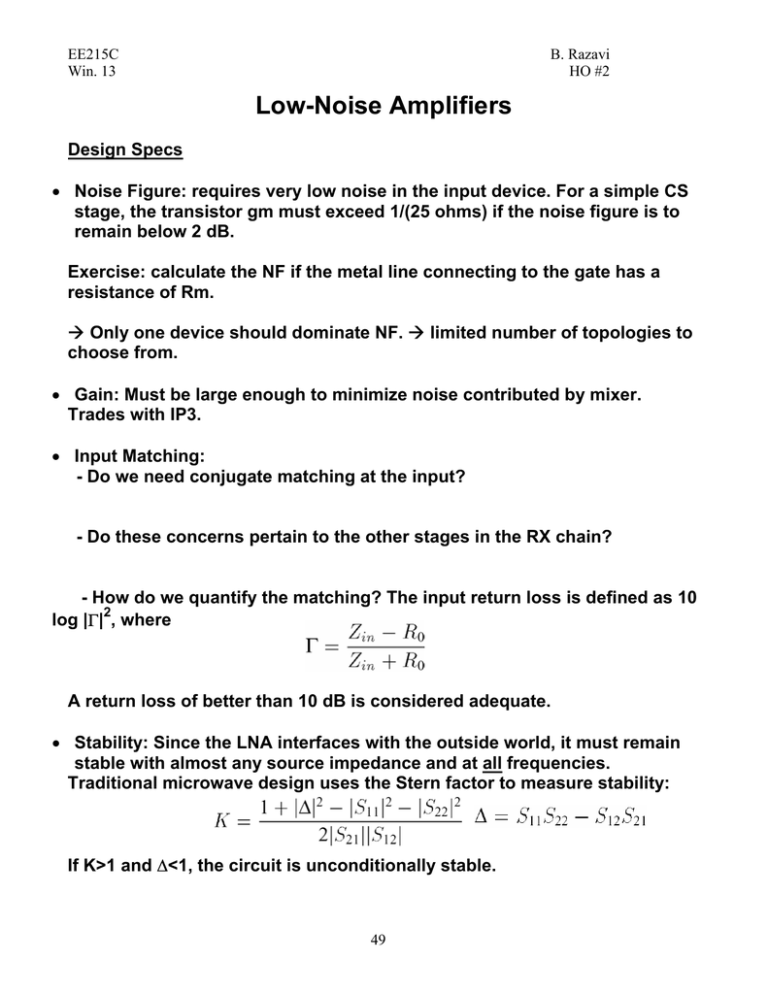
EE215C Win. 13 B. Razavi HO #2 Low-Noise Amplifiers Design Specs • Noise Figure: requires very low noise in the input device. For a simple CS stage, the transistor gm must exceed 1/(25 ohms) if the noise figure is to remain below 2 dB. Exercise: calculate the NF if the metal line connecting to the gate has a resistance of Rm. Æ Only one device should dominate NF. Æ limited number of topologies to choose from. • Gain: Must be large enough to minimize noise contributed by mixer. Trades with IP3. • Input Matching: - Do we need conjugate matching at the input? - Do these concerns pertain to the other stages in the RX chain? - How do we quantify the matching? The input return loss is defined as 10 2 log |Γ| , where A return loss of better than 10 dB is considered adequate. • Stability: Since the LNA interfaces with the outside world, it must remain stable with almost any source impedance and at all frequencies. Traditional microwave design uses the Stern factor to measure stability: If K>1 and ∆<1, the circuit is unconditionally stable. 49 EE215C Win. 13 B. Razavi HO #2 - Complications: Since the LNA output is not matched, S22 becomes rather irrelevant Example: Determine K for a simple CS stage at low frequencies. Conclusion: We design LNAs with high reverse isolation. • Linearity: In most systems, LNAs do not limit the RX linearity. One exception is CDMA. • Bandwidth: The bandwidth must accommodate the entire band specified by the standard. Exercise: An 11a LNA has a 3-dB bandwidth from 5 to 6 GHz. If the LNA load is an inductor, determine the maximum tolerable Q. Problem of Input matching - As explained earlier, the input match cannot be created by tying a physical 50-ohm resistor from input to ground. Exercise: How about tying a parallel inductor that resonates with the input capacitance and also provides a 50-ohm match? Æ Need to create an input resistance of 50 ohms without the noise of a 50ohm resistor. LNA Topologies 50 EE215C Win. 13 B. Razavi HO #2 CS Stage with Inductive Load - Inductor consumes little headroom and resonates with load capacitance. - The input impedance is given by: The can be obtained as: real part - Can choose the values to set the real part to 50 ohms. But it goes negative at lower frequencies. • CS Stage with Resistive Feedback • Common-Gate Stage If we neglect channel-length mod., the low input impedance proves useful here. 51 EE215C Win. 13 B. Razavi HO #2 Exercise: Compute the NF including the noise of the current source and Channel-length modulation. Old Mentality: The tight relationship between the input matching and NF in the CG stage is problematic. We can lower the NF if we allow the input resistance to be higher than Rs. - In deep submicron technologies, the situation changes: Sketch the input resistance vs. freq. If we set the input resistance equal to Rs, Remedy: Add a cascode: But the cascode device contributes some noise and consumes headroom Æ the tail bias has less headroom and more noise. - Design Procedure: (1) Using simulations, plot gm vs. Id for a given W. Pick the Id that gives 80-90% of saturated gm. (“~optimum Id-W combination”) 52 EE215C Win. 13 B. Razavi HO #2 (2) Scale W and Id to obtain 1/(gm + gmb)=50 ohms. (3) Compute necessary value of source inductance. Æ its Rp must be high enough. (4) As a guess, select width of cascode equal to width of input device. (5) Find load inductance to resonate with total output cap. Refer to detailed example in the book. • Cascode CS Stage with Inductive Degeneration - We often need to reduce fT of the transistor to obtain 50 ohms! - But Cgd and the input pad capacitance also lower the real part: It can be proved that the real part falls to: - Also need a series inductor at input: Exercise: A 5-GHz LNA requires an Lg of 2 nH. If the Q is 5, can we build this on-chip? 53 EE215C Win. 13 B. Razavi HO #2 Æ In most cases, both inductors are off-chip. - Computation of Noise Figure - Design Procedure: Start with three knowns: center freq., value of deg. Inductance, value of input series inductance. The following two equations govern the design: (1) Compute Cgs1, gm1, and ωT1 (2) May need to reduce ft. (3) As a guess, choose width of cascode device equal to width of input device (with minimum length). (4) Choose load inductance to resonate with the load cap. (5) Reexamine input match. Refer to example in the book. • Noise-Canceling LNAs Identify two nodes at which signal appears with opposite polarities and noise of input devices with the same polarity. [Bruccoleri, JSSC, Feb.04] 54 EE215C Win. 13 B. Razavi HO #2 How do we choose A1 to ensure noise cancellation? Exercise: Find the NF of the circuit including the input-referred noise voltage of the aux. amplifier. - Implementations: Differential LNAs To achieve a high IP2, direct-conversion receivers may incorporate differential LNAs. But now a “balun” is required: 55

