L2720W
Low drop dual power operational amplifiers
Features
Output current up to 1 A
Operates at low voltages
Single or split supply
Large common-mode and differential-mode
range
Low input-offset voltage
Ground compatible inputs
Low saturation voltage
Thermal shutdown
Clamp diode
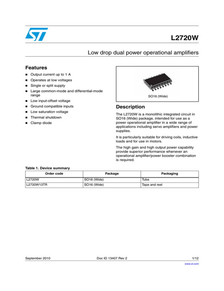
SO16 (Wide)
Description
The L2720W is a monolithic integrated circuit in
SO16 (Wide) package, intended for use as a
power operational amplifier in a wide range of
applications including servo amplifiers and power
supplies.
It is particularly suitable for driving coils, inductive
loads and for use in motors.
The high gain and high output power capability
provide superior performance whenever an
operational amplifier/power booster combination
is required.
Table 1. Device summary
Order code
Package
Packaging
L2720W
SO16 (Wide)
Tube
L2720W13TR
SO16 (Wide)
Tape and reel
September 2010
Doc ID 13407 Rev 2
1/12
www.st.com
12
Connection diagrams
1
L2720W
Connection diagrams
Figure 1.
Figure 2.
Block diagram
VS
1
OUTB
2
N.C.
3
VEE / GND
4
VEE / GND
5
N.C.
6
INB-
7
INB+
8
16 OUTA
15 N.C.
14 N.C.
13 VEE / GND
- +
+ -
12 VEE / GND
11 N.C.
10 INA9 INA+
Schematic diagram (one amplifier)
VS
IN+
OUT
Dump
protection
10pF
IN-
Thermal
protection
VEE / GND
S-9526
2/12
Doc ID 13407 Rev 2
L2720W
2
Pin out
Pin out
Figure 3.
Pin connection (top view)
Table 2.
VS
1
16
OUTA
OUTB
2
15
N.C.
N.C.
3
14
N.C.
VEE / GND
4
13
VEE / GND
VEE / GND
5
12
VEE / GND
N.C.
6
11
N.C.
INB-
7
10
INA-
INB+
8
9
INA+
Pin description
Pin
Name
Type
Description
1
VS
Power
Power supply positive
2
OUTB
Output
Amplifier B output
3
N.C.
-
No internal connection
4
VEE / GND
Power
Power supply negative or ground
5
VEE / GND
Power
Power supply negative or ground
6
N.C.
-
No internal connection
7
INB-
Input
Amplifier B input
8
INB+
Input
Amplifier B input
9
INA+
Input
Amplifier A input
10
INA-
Input
Amplifier A input
11
N.C.
-
No internal connection
12
VEE / GND
Power
Power supply negative or ground
13
VEE / GND
Power
Power supply negative or ground
14
N.C.
-
No internal connection
15
N.C.
-
No internal connection
16
OUTA
Output
Amplifier A output
Doc ID 13407 Rev 2
3/12
Electrical specifications
L2720W
3
Electrical specifications
3.1
Absolute maximum ratings
Table 3.
Absolute maximum ratings
Pin/symbol
3.2
Description
Min
Max
Unit
VS
Supply voltage
-
28
V
VS-PK
Peak supply voltage (50 ms)
-
50
V
Vi
Input voltage range
-
Vs
V
Vi
Differential input voltage range
-
±Vs
V
IO
DC output current
-
1
A
IO-PK
Peak output current (non repetitive)
-
1.5
A
Top
Operating ambient temperature range
-40
125
°C
Tstg, Tj
Storage and junction temperature range
-40
150
°C
Thermal data
Table 4.
Thermal data
Device
Rth j-amb
Rth j-case
Parameter
Min
Thermal resistance junction to ambient (1)
Thermal resistance junction to case pins
(2)
Typ
Max
Unit
-
65
-
°C/W
-
12
-
°C/W
1. On double layer PCB with 4 cm2 copper dissipating area
2. Referred to pins 4, 5, 12 and 13.
3.3
Recommended operating conditions
Table 5.
Recommended operating conditions
Symbol
VS
VE
VIN
4/12
Parameter
Min
Typ
Max
Unit
Positive single power supply
4.0
-
28
V
Positive split power supply
2.0
-
14
V
Negative single power supply
-
0
-
V
Negative split power supply
-2.0
-
-14
V
Input voltage
-
-
VS to
VE
V
Doc ID 13407 Rev 2
L2720W
3.4
Electrical specifications
Electrical characteristics
The electrical specifications in Table 6 below are given for operation under the conditions
VS = 24 V, Tamb = -40 °C to 125 °C and RI connected to GND, unless otherwise specified
Table 6.
Electrical characteristics
Symbol
Parameter
Is
Quiescent current
Iib
Input bias current
Iob
Input offset current
Conditions
Min
Typ
Max
Tamb = 25 °C -
10
15
-
-
10
18
Tamb = 25 °C -
0.2
1
-
0.2
1
Tamb = 25 °C -
-
100
-
-
-
100
Tamb = 25 °C
-10
-
10
-
-10
-
10
VO = VS / 2
VCM = 0
VCM = 0
-
Unit
mA
µA
nA
Vos
Input offset voltage
∆Vos/∆T
Average temperature
coefficient of Vos
-
-
20
-
µV/°
C
SR
Slew rate
Vin = -10 V to +10 V,
RL = 2 kΩ, CL = 100 pF, Av = -1,
Tamb = 25 °C
-
2
-
V/µs
B
Gain-bandwidth product
-
-
1.2
-
MHz
f = 100 Hz
70
80
-
Gv
Open loop voltage gain
f = 1 kHz
-
60
-
CMRR
Common mode rejection ratio
f = 1 kHz
66
84
-
-
70
-
Supply voltage rejection ratio
f = 100 Hz
RG = 10 kΩ
VR = 0.5 V
Vs = 24 V
SVRR
Vs = ±12 V
60
75
-
Tamb = 25 °C -
0.7
1
-
-
0.8
1.5
Tamb = 25 °C -
1.0
1.5
-
-
1.1
1.5
Tamb = 25 °C -
0.3
0.7
-
-
0.4
1
Tamb = 25 °C -
0.5
1
-
-
1.3
1.5
Vs = 24 V
-
60
-
Vs = 6 V
-
60
-
-
10
-
dB
Ip = 100 mA
VDROP(H)
V
Ip = 100 mA
V
Drop voltage low
Ip = 1 A
Cs
Channel separation
eN
Input noise voltage
dB
dB
Drop voltage high
Ip = 1 A
VDROP(L)
mV
f = 1 kHz;
RL = 10 Ω;
Gv = 30 dB
dB
B = 22 Hz to 22 kHz,
Tamb = 25 °C
Doc ID 13407 Rev 2
µV
5/12
Electrical specifications
Table 6.
L2720W
Electrical characteristics (continued)
Symbol
Parameter
Conditions
Min
Typ
Max
Unit
IN
Input noise current
B = 22 Hz to 22 kHz,
Tamb = 25 °C
-
200
-
pA
φm
Phase margin
RL = 2 kΩ, CL = 100 pF,
Tamb = 25 °C
-
65
-
°C
Am
Gain margin
RL = 2 kΩ, CL = 100 pF,
Tamb = 25 °C
-
15
-
dB
3.5
6/12
Characterization curves
Figure 4.
Quiescent current vs supply current
Figure 5.
Open loop gain vs frequency
Doc ID 13407 Rev 2
L2720W
Electrical specifications
Figure 6.
Common mode rejection vs frequency
Figure 7.
Output swing vs load current (Vs = ±5 V)
Figure 8.
Output swing vs load current (Vs = ±12 V)
Doc ID 13407 Rev 2
7/12
Electrical specifications
Figure 9.
L2720W
Supply voltage rejection vs frequency
Figure 10. Channel separation vs frequency
Figure 11. Voltage gain and phase vs frequency
Fig.8 Voltage Gain and Phase vs Freq
Gv (dB)
80
70
60
Vs=24V
Rl = 2 k?
50
40
30
20
10
0
-10
-20
1
8/12
10
100
f (KHz)
Doc ID 13407 Rev 2
1000
80 Phase(°)
-80
90
-90
100
-100
110
-110
120
-120
130
-130
10000
L2720W
Electrical specifications
Figure 12. Phase margin vs output load capacitance
Phase margin (degrees)
70
60
50
Vs = ±12 V
R1 = 2 KΩ
40
30
20
0
0.4
0.8
Doc ID 13407 Rev 2
1.2
1.6
2
9/12
Package mechanical data
4
L2720W
Package mechanical data
In order to meet environmental requirements, ST offers these devices in different grades of
ECOPACK® packages, depending on their level of environmental compliance. ECOPACK®
specifications, grade definitions and product status are available at: www.st.com.
ECOPACK® is an ST trademark.
Figure 13. SO16 (Wide) mechanical data and package dimensions
mm
inch
DIM.
MIN.
TYP.
MAX.
MIN.
TYP.
MAX.
A
2.35
-
2.65
0.093
-
0.104
A1
0.10
-
0.30
0.004
-
0.012
B
0.33
-
0.51
0.013
-
0.200
0.23
-
0.32
0.009
-
0.013
10.10
-
10.50
0.398
-
0.413
E
7.40
-
7.60
0.291
-
0.299
e
-
1.27
-
-
0.050
-
H
10.0
-
10.65
0.394
-
0.419
h
0.25
-
0.75
0.010
-
0.030
L
0.40
-
1.27
0.016
-
0.050
-
0.004
C
D
(1)
k
ddd
OUTLINE AND
MECHANICAL DATA
0° (min.), 8° (max.)
-
-
0.10
-
(1) “D” dimension does not include mold flash, protusions or gate
burrs. Mold flash, protusions or gate burrs shall not exceed
0.15mm per side.
SO16 (Wide)
0016021 C
10/12
Doc ID 13407 Rev 2
L2720W
5
Revision history
Revision history
Table 7.
Document revision history
Date
Revision
Changes
04-Apr-2007
1
Initial release.
03-Sep-2010
2
Complete update and change in presentation
Doc ID 13407 Rev 2
11/12
L2720W
Please Read Carefully:
Information in this document is provided solely in connection with ST products. STMicroelectronics NV and its subsidiaries (“ST”) reserve the
right to make changes, corrections, modifications or improvements, to this document, and the products and services described herein at any
time, without notice.
All ST products are sold pursuant to ST’s terms and conditions of sale.
Purchasers are solely responsible for the choice, selection and use of the ST products and services described herein, and ST assumes no
liability whatsoever relating to the choice, selection or use of the ST products and services described herein.
No license, express or implied, by estoppel or otherwise, to any intellectual property rights is granted under this document. If any part of this
document refers to any third party products or services it shall not be deemed a license grant by ST for the use of such third party products
or services, or any intellectual property contained therein or considered as a warranty covering the use in any manner whatsoever of such
third party products or services or any intellectual property contained therein.
UNLESS OTHERWISE SET FORTH IN ST’S TERMS AND CONDITIONS OF SALE ST DISCLAIMS ANY EXPRESS OR IMPLIED
WARRANTY WITH RESPECT TO THE USE AND/OR SALE OF ST PRODUCTS INCLUDING WITHOUT LIMITATION IMPLIED
WARRANTIES OF MERCHANTABILITY, FITNESS FOR A PARTICULAR PURPOSE (AND THEIR EQUIVALENTS UNDER THE LAWS
OF ANY JURISDICTION), OR INFRINGEMENT OF ANY PATENT, COPYRIGHT OR OTHER INTELLECTUAL PROPERTY RIGHT.
UNLESS EXPRESSLY APPROVED IN WRITING BY AN AUTHORIZED ST REPRESENTATIVE, ST PRODUCTS ARE NOT
RECOMMENDED, AUTHORIZED OR WARRANTED FOR USE IN MILITARY, AIR CRAFT, SPACE, LIFE SAVING, OR LIFE SUSTAINING
APPLICATIONS, NOR IN PRODUCTS OR SYSTEMS WHERE FAILURE OR MALFUNCTION MAY RESULT IN PERSONAL INJURY,
DEATH, OR SEVERE PROPERTY OR ENVIRONMENTAL DAMAGE. ST PRODUCTS WHICH ARE NOT SPECIFIED AS "AUTOMOTIVE
GRADE" MAY ONLY BE USED IN AUTOMOTIVE APPLICATIONS AT USER’S OWN RISK.
Resale of ST products with provisions different from the statements and/or technical features set forth in this document shall immediately void
any warranty granted by ST for the ST product or service described herein and shall not create or extend in any manner whatsoever, any
liability of ST.
ST and the ST logo are trademarks or registered trademarks of ST in various countries.
Information in this document supersedes and replaces all information previously supplied.
The ST logo is a registered trademark of STMicroelectronics. All other names are the property of their respective owners.
© 2010 STMicroelectronics - All rights reserved
STMicroelectronics group of companies
Australia - Belgium - Brazil - Canada - China - Czech Republic - Finland - France - Germany - Hong Kong - India - Israel - Italy - Japan Malaysia - Malta - Morocco - Philippines - Singapore - Spain - Sweden - Switzerland - United Kingdom - United States of America
www.st.com
12/12
Doc ID 13407 Rev 2


