Solar nanocomposites with complementary charge extraction
advertisement
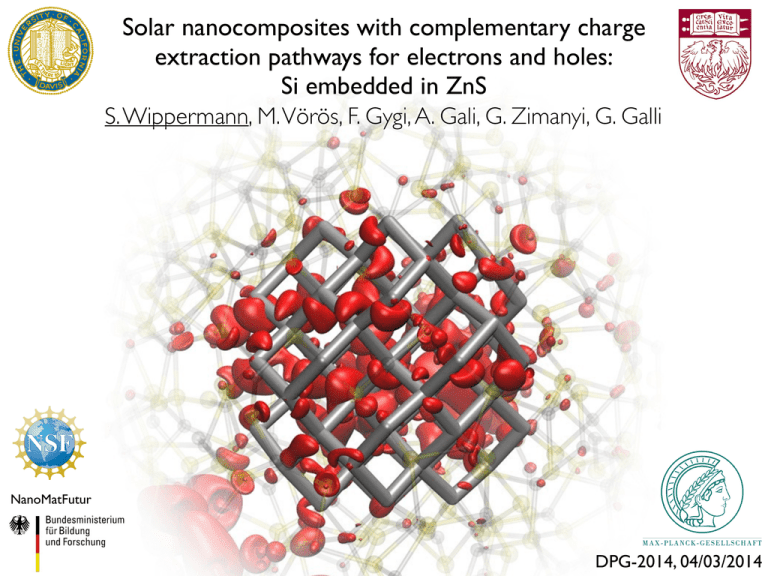
Solar nanocomposites with complementary charge extraction pathways for electrons and holes: Si embedded in ZnS S. Wippermann, M. Vörös, F. Gygi, A. Gali, G. Zimanyi, G. Galli NanoMatFutur DPG-2014, 04/03/2014 Search for materials to harvest light Nanocomposites based on Si nanocrystals embedded in a charge transport matrix are promising candidates for light absorbers in quantum dot based 3rd generation photovoltaics architectures d = 3.3nm Si nanocrystals in SiO2 [M. Zacharias et al., Appl. Phys. Lett. 80, 661 (2002)] Search for materials to harvest light Nanocomposites based on Si nanocrystals embedded in a charge transport matrix are promising candidates for light absorbers in quantum dot based 3rd generation photovoltaics architectures d = 3.3nm Si nanocrystals in SiO2 Key problems: ! Ensure efficient charge transport and low recombination rates ! Understand interplay between interface structure, quantum-confinement, defects [M. Zacharias et al., Appl. Phys. Lett. 80, 661 (2002)] Search for materials to harvest light Nanocomposites based on Si nanocrystals embedded in a charge transport matrix are promising candidates for light absorbers in quantum dot based 3rd generation photovoltaics architectures d = 3.3nm Si nanocrystals in SiO2 Key problems: ! Ensure efficient charge transport and low recombination rates ! Understand interplay between interface structure, quantum-confinement, defects Si nanocrystals in ZnS: ! ZnS is earth-abundant, non-toxic and features a favourable band-alignment with Si at least for planar heterointerfaces ! Investigate Si-ZnS nanocomposites from first principles [M. Zacharias et al., Appl. Phys. Lett. 80, 661 (2002)] Embedding Si nanocrystals in a-ZnS Create structural models for a-ZnS embedded Si35, Si66, Si123, Si172 nanoparticles (NPs): replace spherical region (1.1 - 1.9 nm) in 4x4x4 ZnS unit cell and amorphize ZnS matrix using ab initio molecular dynamics (MD) ! DFT-LDA (Qbox) EC = 80 Ry, τ = 2 fs, T = 2400 K, Si atoms free to move for T < 600 K, 10-20 ps MD Si123 (1.6nm) Embedding Si nanocrystals in a-ZnS Create structural models for a-ZnS embedded Si35, Si66, Si123, Si172 nanoparticles (NPs): replace spherical region (1.1 - 1.9 nm) in 4x4x4 ZnS unit cell and amorphize ZnS matrix using ab initio molecular dynamics (MD) ! DFT-LDA (Qbox) EC = 80 Ry, τ = 2 fs, T = 2400 K, Si atoms free to move for T < 600 K, 10-20 ps MD Si123 (1.6nm) Different starting geometries, equilibration & cooling times lead to very similar structures Formation of sulfur-shell on Si-NP surface observed ! => Examine interface structure Sulfur shell formation introduces new mid-gap states 3-fold coordinated interfacial sulfur: achieves noble gas state with 1 S-Si, 2 S-Zn bonds and 1 lone pair 1/2 1/2 3/2 2 3/2 S lone pair 1 1 Si NP-surface 1 1 1 Sulfur shell formation introduces new mid-gap states 3-fold coordinated interfacial sulfur: achieves noble gas state with 1 S-Si, 2 S-Zn bonds and 1 lone pair Lone pairs of 3-fold coordinated sulfur at NP-matrix interface introduce new occupied mid-gap states, HOMO and near-HOMO states involve lone pairs Si35 NP HOMO 1/2 1/2 3/2 2 3/2 S lone pair 1 1 Si NP-surface 1 1 1 Sulfur shell formation introduces new mid-gap states 3-fold coordinated interfacial sulfur: achieves noble gas state with 1 S-Si, 2 S-Zn bonds and 1 lone pair Lone pairs of 3-fold coordinated sulfur at NP-matrix interface introduce new occupied mid-gap states, HOMO and near-HOMO states involve lone pairs => pronounced gap-reduction of embedded NPs Si35 NP HOMO 1/2 1/2 3/2 2 3/2 S lone pair 1 1 Si NP-surface 1 1 1 Si nanoparticles (NPs) in SiO2: type I junction Si NPs embedded in SiO2 form a type I junction with their silica host Valence and conduction band edges localized inside Si NP => no charge transport ! NP LUMO may be pushed above SiO2 CBM by compressive strain [T. Li, F. Gygi, G. Galli, PRL 2011] valence band edge SiO2 CBM Si NP LUMO Si NP HOMO SiO2 VBM conduction band edge Si nanoparticles (NPs) in ZnS: type II junction Si NPs in ZnS form a type II junction at equilibrium density ! Charge-separated transport channels for electrons and holes may facilitate charge extraction and suppress recombination ! Hole transport through host matrix, highly desirable for solar cells valence band edge ZnS CBM Si NP LUMO ZnS VBM Si NP HOMO conduction band edge Si nanoparticles in ZnS: band alignment Calculate band edge energies as a function of the radial distance from the center of the NP Si123 in Zn188S201 ZnS CBM Si NP LUMO ZnS VBM Si NP HOMO ! DFT-LDA band offsets reliable? ! => calculate band offsets in GW approximation Formation of type II interface between Si NP and a-ZnS matrix, if, and only if, sulfur content is above a certain threshold GW for large systems ! Calculation, storage & inversion of dielectric matrix ε is major computational bottleneck => spectral representation of ε (RPA) N N ˜= ṽi i ṽiH = i=1 ṽi ( i 1)ṽiH + I i=1 [4] H.-V. Nguyen, T. A. Pham, D. Rocca, G. Galli, PRB 85 081101 (2012), PRB 87, 155148 (2013) GW for large systems ! Calculation, storage & inversion of dielectric matrix ε is major computational bottleneck => spectral representation of ε (RPA) N N ˜= ! ṽi i ṽiH = i=1 ṽi ( i 1)ṽiH + I i=1 Calculating eigenvectors/-values does NOT require explicit knowledge of the matrix itself; knowing the action of ε on an arbitrary vector is sufficient ! I) VSCF = vc n In linear response: ( Charge density response n to perturbation of self-consistent field be evaluated from density functional perturbation theory VSCF can [4] H.-V. Nguyen, T. A. Pham, D. Rocca, G. Galli, PRB 85 081101 (2012), PRB 87, 155148 (2013) GW for large systems ! Calculation, storage & inversion of dielectric matrix ε is major computational bottleneck => spectral representation of ε (RPA) N N ˜= ! ṽi i ṽiH = i=1 ṽi ( i 1)ṽiH + I i=1 Calculating eigenvectors/-values does NOT require explicit knowledge of the matrix itself; knowing the action of ε on an arbitrary vector is sufficient ! I) VSCF = vc n In linear response: ( Charge density response n to perturbation of self-consistent field be evaluated from density functional perturbation theory Orthogonal iteration procedure to obtain eigen- vector/-value pairs, using VSCF as trial potentials VSCF can In RPA fast monotonous decay of dielectric eigenvalue spectrum ! Single parameter Neig to control numerical accuracy ! No summation over empty states, no inversion [4] H.-V. Nguyen, T. A. Pham, D. Rocca, G. Galli, PRB 85 081101 (2012), PRB 87, 155148 (2013) GW for large systems ! ! Calculation, storage & inversion of dielectric matrix ε is major computational bottleneck => spectral representation of ε (RPA) N N D. Rocca, H.-V. Nguyen, T. A. Pham (UCD) ˜= ṽi i ṽiH = ṽi ( i 1)ṽiH + I i=1 i=1 Calculating eigenvectors/-values does NOT require explicit knowledge of the matrix itself; knowing the action of ε on an arbitrary vector is sufficient ! I) VSCF = vc n In linear response: ( Charge density response n to perturbation of self-consistent field be evaluated from density functional perturbation theory Orthogonal iteration procedure to obtain eigen- vector/-value pairs, using VSCF as trial potentials VSCF can In RPA fast monotonous decay of dielectric eigenvalue spectrum ! Single parameter Neig to control numerical accuracy ! No summation over empty states, no inversion [4] H.-V. Nguyen, T. A. Pham, D. Rocca, G. Galli, PRB 85 081101 (2012), PRB 87, 155148 (2013) Band alignment from many body perturbation theory (GW) ! GW calculations possible for a system as large as Si35Zn81S100 Band alignment from many body perturbation theory (GW) ! ! GW calculations possible for a system as large as Si35Zn81S100 Many body corrections in GW approximation introduce mainly a rigid shift => confirms type II alignment Summary Investigated 1.1 - 1.9 nm Si nanocrystals embedded in a-ZnS using ab initio MD and quasiparticle calculations in GW approximation ! ZnS-embedded Si nanocrystals form a type II junction with the ZnS host in sulfur-rich conditions ! Band edges localized in different portions of nanocomposite => charge- separated transport channels for electrons and holes Acknowledgements Giulia Galli and her group at UChicago, especially Marton Vörös and Tuan Anh Pham Francois Gygi (UC Davis), Gergely Zimanyi (UC Davis), Adam Gali (Budapest Univ.), Dario Rocca (Univ. Lorraine) NanoMatFutur 13N12972 Wi3879/1-1 NISE-project 35687 NSF/Solar DMR-1035468 Max-Planck-Institute for Iron Research, Düsseldorf Band alignments of semiconductors C. Van de Walle, J. Neugebauer, Nature 423, 626 (2003) Band alignments of semiconductors C. Van de Walle, J. Neugebauer, Nature 423, 626 (2003) Band alignments of semiconductors C. Van de Walle, J. Neugebauer, Nature 423, 626 (2003) Band alignments of semiconductors C. Van de Walle, J. Neugebauer, Nature 423, 626 (2003) Band alignments of semiconductors C. Van de Walle, J. Neugebauer, Nature 423, 626 (2003)

