Automotive Electronics
Product Information
Lambda Probe Interface IC - CJ125
Customer benefits:
Excellent system know-how
Smart concepts for system safety
Secured supply
Long- term availability of manufacturing processes
and products
QS9000 and ISO/TS16949 certified
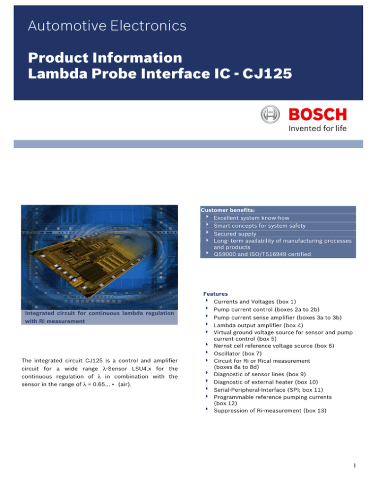
Integrated circuit for continuous lambda regulation
with Ri measurement
Features
Currents and Voltages (box 1)
Pump current control (boxes 2a to 2b)
Pump current sense amplifier (boxes 3a to 3b)
Lambda output amplifier (box 4)
Virtual ground voltage source for sensor and pump
current control (box 5)
Nernst cell reference voltage source (box 6)
Oscillator (box 7)
The integrated circuit CJ125 is a control and amplifier
circuit for a wide range λ-Sensor LSU4.x for the
continuous regulation of λ in combination with the
sensor in the range of λ = 0.65... • (air).
Circuit for Ri or Rical measurement
(boxes 8a to 8d)
Diagnostic of sensor lines (box 9)
Diagnostic of external heater (box 10)
Serial-Peripheral-Interface (SPI; box 11)
Programmable reference pumping currents
(box 12)
Suppression of Ri-measurement (box 13)
1
Block-/ functional diagram
Application circuit (only proposal!)
2
PIN configuration
SOIC24
The application circuit of the CJ125 consists of the
following parts:
Capacitor between [VCC] and [GND] to stabilize
the supply voltage VCC
Capacitor between [UB] and [GND] to stabilize
the supply voltage VUB
Capacitor between [CF] and [GND] to filter the
lambda signal
Capacitor between [UA] and [GND] to stabilize
lambda signal output
Capacitor between [UN] and [GND] to stabilize
nernst signal
Capacitor between [/RST] and [GND] to stabilize
reset signal
Shunt between [IA] and [IP] for pump current
sensing
Resistor between [IA] and [UP] to compensate
parasitic effects of the lambda sensor
Resistor between [US] and [UP] to feed the nernst
cell reference voltage into the pump current control
circuit
Resistor between [UP] and [UN] for leakage
detection
Resistor between [RF] and [CF] to filter the lambda
signal
Capacitor between [UR] and [GND] to stabilize
the output signal for ADC
Capacitor between [UN] and [GND] for filtering
Resistor between [RM] and capacitor at [CM] for
adjustment of Ri measurement current
Capacitor between [CM] and resistance at [RM] for
DC filtering
Resistor between [RS] and [VM] for adjustment
Resistor between [DIAHD] and Drain of the external
heater
Resistor and capacitor before [UN] for filtering
PLCC28
LQFP32
3
Pin description
Pin
Description
Pin
Description
UB
VCC, VCCSa)
GND, GNDSb)
VM
Power supply input (14V)
Power supply input (5V)
Ground
Virtual ground of pump current control and
of the LSU (0.5VCC)
Nernst cell reference voltage (450mV)
Inverting input of pump current amplifier
(shunt voltage)
Non inverting input of pump current
amplifier and output of the pump current
control
Output of pump current amplifier
(-> external filter)
Input of lambda output amplifier (after
external filter)
Output of lambda output amplifier
Non inverting input of pump current control
Inverting input of pump current control
respective in-/output for Ri-measurement
(LSU)
RM
CM
RS
UR
DIAHG
DIAHD
Output Ri-measurement current (DC)
Input Ri-measurement current (AC, DC free)
In-/output Ri-calibration measurement
Output Ri-signal (analogous)
Diagnosis input (gate of external transistor)
Diagnosis input (drain of external
transistor)
Input SPI-clock (from µC)
Input serial data (SPI, from µC)
Output serial data (SPI, to µC)
Slave select (SPI, from µC)
Input Reset
Rextern = 10kΩ
US
IP
IA
RF
CF
UA
UP
UN
SCK
SI
SO
/SS
/RST
OSZ
a.)
For hybrid version it is recommended to connect VVCS with
the reference VCC for the ADC
b.)
For hybrid version it is recommended to connect GNDS
with the reference ground for the ADC
Maximum Ratings
Parameter
Condition
Supply voltage UB
Supply voltage VCC
Temperature
junction
storage
ambient for SOIC/PLCC
for max 50h
ambient for LQFP
for max 50h
Maximum allowed voltages valid
for pins:
RM, UP, US,RF, CF, UA, UR,
DIAHG, DIAHD; SCK, SI, SO, /SS,
/RST, OSZ
Allowed current
Maximum allowed voltages,
no destruction when ISO-pulses
3a,b are applied.
Valid for board pins: RS, UN, VM,
IA, IP, CM
Offset between GND and GNDS
Offset between VCC and VCCS
ESD
ext. resistor 6.8 kΩ
Human Body Model
R=1.5kΩ, C=100pF
Symbol
Min.
Max.
Unit
VUB
VVCC
TJ
TST
TA
-0.3
-0.3
-40
-40
-40
-40
VX
-0.3
35
5.5
150
150
110
125
125
140
VVCC + 0.3
V
V
°C
°C
°C
°C
°C
°C
V
IDIAHD
VX
-1
-0.3
10
28
mA
V
∆VGND
∆VVCC
-0.25
-0.25
-2
0.25
0.25
2
V
V
kV
4
Electrical Characteristics
Parameter
Power Supply
Power supply
Operating range
Current consumption
Current consumption
Pump current control
Offset voltage
Input current
Input offset current
Condition
Symbol
Min.
Max.
Unit
VGND = VGNDS
VVCC = VVCCS
VUB
VVCC
IVCC
IVCCS
9
4.75
18
5.25
76
4
V
V
mA
mA
-10
-1
-1
10
1
1
mV
µA
µA
10
30
mA
Voff
-40°C • Tj < 150°C
IUP, UN
-40°C • Tj < 150°C
Ioff
VUN < VUP; PA = 1;
Output current source condition
-IA
0.5V < VIA < VCC-0.5V
VUN > VUP; PA = 1;
Output current sink condition
IA
0.6V < VIA < VCC-0.5V
No output current
PA = 0
IA
Pump current sense amplifier (LA = 0: measurement mode; LA = 1: adjustment mode)
Input current
-40°C • Tj < 150°C
IIP
Amplification
SPI-bit VL = 1
A0
Amplification
SPI-bit VL = 0
A0
CMRR-1
CMRR-1= ∆VUA/ ∆VIP
VIP=VIA=1...4V
Common mode rejection ratio
0.5V < VUA < VCC-0.5V
| IUA | < 10µA
Output voltage swing
| IUA | < 10µA; LA = 0
VUA
Output voltage adjustment
IRF =0µA; LA = 1
VFR/ VVCC
•VUA
∆VUA=VUA (LA = 1) - VUA(LA = 0)
Output error offset adjust
VIP=VIA=VVM
| IUA | < 10µA
Virtual ground voltage source
Output current operating range
IVM
Output voltage ratio
-IIA-1mA < IVM < -IIA +1mA
VVM/ VVCC
Nernst cell reference voltage source
Output current operating range
IUS
Oscillator
Frequency
f
external 10kΩ
Measurement current for Ri (RA = 0 measurement mode; RA =1 adjustment mode)
Output resistor of push-pull-stage
-1mA • IRM • 1mA
R
Ri amplifier
Leakage current when switch is open
ILEAK
Amplification
A0
Ron for a switch
Ron
Input voltage range at CM, UN and RS
VRI
Output voltage range
VUR
Zero point for output trace
VUR/ VVCC
Pump reference current
programmable with SPI-bits
Current range
- IUn
PRx; x = 0 to 3
Diagnosis of sensor lines
Short circuit to ground
VVM / VVCC
Short circuit to Vbat
VVM / VVCC
Short circuit to ground
VUN / VVCC
Short circuit to Vbat
VUN / VVCC
Short circuit to ground
VIA,IP
Short circuit to Vbat
VIA
Diagnosis of external heater
Low level
VDIAHG
High level
VDIAHG
Input current (no pull up!)
- IDIAHG
Short circuit to ground
DIAHG = low
IDIAHD
Short circuit to Vbat
DIAHG = high
IDIAHD
Open load
DIAHG = low
IDIAHD
No failure
DIAHG = high
IDIAHD
No failure
DIAHG = low
IDIAHD
Filter time
T=1/f
tDIAG / T
SPI
Data rate
Bit-frame
Number of read / write commands
Number of register
10
30
mA
-10
10
µA
-1
16.62
7,82
1
17.24
8.15
12
µA
mV/V
0.20
0.285
-3
VVCC -0.18
0.315
3
-IIA -2
0.48
-IIA +2
0.52
mA
-0.4
0.4
mA
2.49
3.51
kHz
5
200
Ω
-500
15
nA
2
0.06 VVCC
0.05
500
16.3
200
VVCC -1.1
VVCC – 0.2
0.063
0
150
µA
0.35
0.55
0.30
0.72
0.3
VVCC
0.45
0.65
0.40
0.88
1.5
VVCC + 2
V
V
-0.3
0.7 VVCC
-1
-1000
-100
-100
-1000
350
30 / 32
0.3 VVCC
VVCC + 0.3
1
-350
10 000
100
-350
10 000
32 / 32
2
16
6
4
V
mV
Ω
V
V
V
V
µA
µA
µA
µA
µA
µA
Mbaud
bit
5
SPI - Block schematic, register, RD / WR-commands with hec- code
Failure bitsa)
00
01
10
1 1d)
Ext. heater
Sensorb)
Short circuit to
ground
Open load
Short circuit to Vbat
No failure
Short circuit to
ground
Low battery c)
Short circuit to Vbat
No failure
SPI – Write Access
a)
Only each failure of the sensor leads to a switch off of
pump current and virtual ground
b) Failure identification at UN must be enabled with
ENSCUN
c) Open load is not recognizable; bits used for low
battery
d) After RD_DIAG or if no failure is present; Failure bits
will be restored if failure is still present
SPI - Timing
v: command valid/not valid; dc: don’t care („-“)
x: 0 or 1; Z: tristate
SPI – Read Access
6
Chipset
x
Battery
CY320
Sensor
Sensor
Sensor
CAN
System Supply
µC Supply
Sensor Supply
Watchdog
Reset
CAN Driver
ISO Interface
Sleep/Wake
ISO
8
8x
e.g.
LEDs
_
+
CY100
2
Fela
ISO
µC
e.g.
Infineon
TC1796
A/D
RAM
CAN
Peripherals
FLASH
Valves
CJ945
18 Low Side
Power Drivers
6x
6x
2x
4x
2A/70V
2A/45V
3A/45V
1A/45V
x
Relays
x
Inductivities
x
Resistors
x
_
+
Fela
CK240
Lamps
x
Ignition Drivers
8x 10 Bit A/D 5V
Small Signal Out
ISO Interface
H-Bridge
Concept
FLASH
CY30
CF173
RPM
CAN Driver
CJ840
SMD085
CJ125
Direct Injection
Pressure Sensor
λ-Sensor Control
CAN
Contact
Robert Bosch GmbH
Sales Semiconductors
Postbox 13 42
72703 Reutlingen
Germany
Tel.: +49 7121 35-2979
Fax: +49 7121 35-2170
Robert Bosch Corporation
Component Sales
38000 Hills Tech Drive
Farmington Hills, MI 48331
USA
Tel.: +1 248 876-7441
Fax: +1 248 848-2818
E-Mail: bosch.semiconductors@de.bosch.com
Robert Bosch K.K.
Component Sales
9-1, Ushikubo 3-chome
Tsuzuki-ku, Yokohama 224
Japan
Tel.: +81 45 9 12-83 01
Fax: +81 45 9 12-95 73
Internet: www.bosch-semiconductors.de
© 04/2006 All rights reserved by Robert Bosch GmbH including the right to file industrial property rights
Robert Bosch GmbH retains the sole powers of distribution, such as reproduction, copying and distribution.
For any use of products outside the released application, specified environments or installation conditions no warranty shall apply
and Bosch shall not be liable for such products or any damage caused by such products.
7


