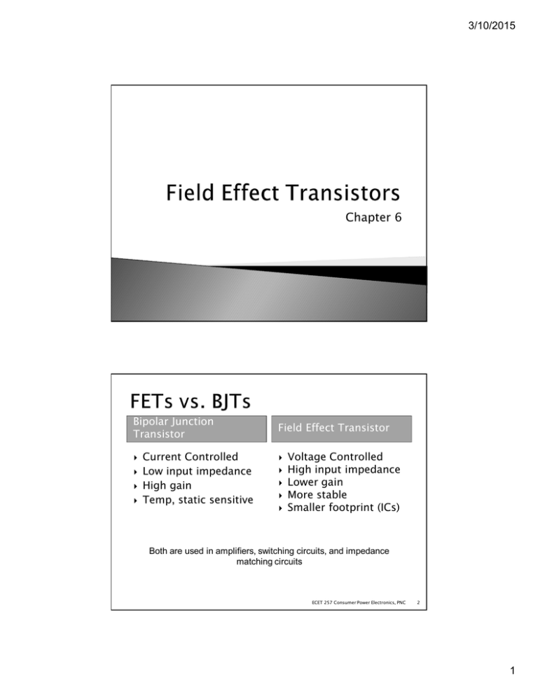
Ch. 6 Field Effect Transistors
advertisement

3/10/2015 Chapter 6 Bipolar Junction Transistor Current Controlled Low input impedance High gain Temp, static sensitive Field Effect Transistor Voltage Controlled High input impedance Lower gain More stable Smaller footprint (ICs) Both are used in amplifiers, switching circuits, and impedance matching circuits ECET 257 Consumer Power Electronics, PNC 2 1 3/10/2015 JFET: Junction FET MOSFET: Metal–Oxide–Semiconductor FET D-MOSFET: Depletion MOSFET E-MOSFET: Enhancement MOSFET ECET 257 Consumer Power Electronics, PNC 3 Two main types ◦ N-channel (more common) ◦ P-channel Three terminals ◦ Drain ◦ Source ◦ Gate ECET 257 Consumer Power Electronics, PNC 4 2 3/10/2015 The source is the accumulation of electrons at the negative pole of the drain-source voltage. The drain is the electron deficiency (or holes) at the positive pole of the applied voltage. The gate controls the width of the nchannel and, therefore, the flow of charges from source to drain. LABELS BASED ON ELECTRON FLOW ECET 257 Consumer Power Electronics, PNC 5 There are three basic operating conditions for a JFET: • VGS = 0 V, VDS increasing to some positive value • VGS < 0 V, VDS at some positive value • Voltage-controlled resistor ECET 257 Consumer Power Electronics, PNC 6 3 3/10/2015 Three things happen when VGS = 0 V and VDS increases from 0 V to a more positive voltage: • The size of the depletion region between p- type gate and n-channel increases. • Increasing the size of the depletion region decreases the width of the nchannel, which increases its resistance. • Even though the n-channel resistance is increasing, the current from source to drain (ID) through the n-channel is increasing because VDS is increasing. ECET 257 Consumer Power Electronics, PNC 7 Depletion ranges grow till Vp ◦ ID reaches saturation (IDSS) ◦ No increase in ID with VDS increases ECET 257 Consumer Power Electronics, PNC 8 4 3/10/2015 Depletion region grows as VGS becomes more negative Reaches IDSS at a lower level ECET 257 Consumer Power Electronics, PNC 9 As VGS becomes more negative: • The JFET experiences pinch-off at a lower voltage (VP). • ID decreases (ID < IDSS) even when VDS increases • ID eventually drops to 0 A. The value of VGS that causes this to occur is designated VGS(off). ECET 257 Consumer Power Electronics, PNC 10 5 3/10/2015 The region to the left of the pinch-off point is called the ohmic region. The JFET can be used as a variable resistor, where VGS controls the drain-source resistance (rd). As VGS becomes more negative, the resistance (rd) increases. ECET 257 Consumer Power Electronics, PNC 11 P and N channel JFETs operate the same ◦ Voltage polarities and current directions are reversed. ECET 257 Consumer Power Electronics, PNC 12 6 3/10/2015 As VGS becomes more positive: • The JFET experiences pinch-off at a lower voltage (VP). • The depletion region increases, and ID decreases (ID < IDSS) • ID eventually drops to 0 A (when VGS = VGSoff) Also note that at high levels of VDS the JFET reaches a breakdown situation: ID increases uncontrollably if VDS > VDSmax. ECET 257 Consumer Power Electronics, PNC 13 ECET 257 Consumer Power Electronics, PNC 14 P-channel symbol has the arrows reversed 7 3/10/2015 JFET input-to-output transfer characteristics are not as straightforward as they are for a BJT. • BJT: indicates the relationship between IB (input) and IC (output). • JFET: The relationship of VGS (input) and ID (output) : Shockley’s equation ECET 257 Consumer Power Electronics, PNC 15 Final version with limits shown on Pg. 393 ECET 257 Consumer Power Electronics, PNC 16 8 3/10/2015 Manually Solve for VGS = 0 V: ◦ ID = IDSS Graphing Calculator Solving for VGS = VGS(off): Solving for VGS = Vp/2: ◦ = 1− ◦ IDSS is in mA (enter without e-3) ◦ Set view window for proper view ◦ ID = 0 A Plot 1 = Trace graph ◦ X=VGS ◦ Y=ID Draw curve P-channel is drawn the same, except VP and VGS are positive, and the curve is mirrored over the y-axis ECET 257 Consumer Power Electronics, PNC 17 Given: IDSS = 8 mA VP = -4 V Draw transfer curve Find VGS when ID = 2.5 mA ECET 257 Consumer Power Electronics, PNC 18 9 3/10/2015 Electrical Characteristics ECET 257 Consumer Power Electronics, PNC 19 ECET 257 Consumer Power Electronics, PNC 20 Maximum Ratings 10 3/10/2015 ECET 257 Consumer Power Electronics, PNC = ID=IS IG≅ 0 A FET 1− 21 IC=βIB IC ≅ IE VBE = 0.7 BJT ECET 257 Consumer Power Electronics, PNC 22 11 3/10/2015 ECET 257 Consumer Power Electronics, PNC 23 Metal Oxide Semiconductor Field Effect Transistor ◦ Metal – D, G, and S connections ◦ Oxide – SiO2 insulation layer ◦ May also be called IGFET (insulated gate FET) Two main types ◦ Depletion ◦ Enhancement ECET 257 Consumer Power Electronics, PNC 24 12 3/10/2015 The Drain (D) and Source (S) connect to the to n-type regions. These n-typed regions are connected via an n-channel. This n-channel is connected to the Gate (G) via a thin insulating layer of silicon dioxide (SiO2). The n-type material lies on a ptype substrate that may have an additional terminal connection called the Substrate (SS). ECET 257 Consumer Power Electronics, PNC 25 ECET 257 Consumer Power Electronics, PNC 26 13 3/10/2015 The characteristics are similar to a JFET. When VGS = 0 V, ID = IDSS When VGS < 0 V, ID < IDSS The formula used to plot the transfer curve for a JFET applies to a D-MOSFET as well: ECET 257 Consumer Power Electronics, PNC 27 VGS > 0 V, ID increases above IDSS (ID > IDSS) ◦ Free electrons are pulled from the P-channel ◦ Very easy to exceed IDMAX ◦ Still plotted using Shockley’s equation ECET 257 Consumer Power Electronics, PNC 28 14 3/10/2015 Given: ◦ IDSS = 10 mA ◦ VP = -4 Draw transfer curve Find ID when VGS = -2 V Find ID when VGS = 1 V ECET 257 Consumer Power Electronics, PNC 29 ECET 257 Consumer Power Electronics, PNC 30 15 3/10/2015 ECET 257 Consumer Power Electronics, PNC 31 ECET 257 Consumer Power Electronics, PNC 32 Maximum Ratings 16 3/10/2015 Electrical Characteristics ECET 257 Consumer Power Electronics, PNC 33 The Drain (D) and Source (S) connect to the to n-type regions. These n-type regions are connected via an n-channel The Gate (G) connects to the p-type substrate via a thin insulating layer of silicon dioxide (SiO2) There is no channel The n-type material lies on a p-type substrate that may have an additional terminal connection called the Substrate (SS) ECET 257 Consumer Power Electronics, PNC 34 17 3/10/2015 Operates only in enhancement mode ◦ When = 0 ≥ 0, ◦ When 0 < < , = 0 ◦ When , > 0 ≥ Increases in VDS cause ID to increase till IDSAT ECET 257 Consumer Power Electronics, PNC To find current k- use given conditions and VT of MOSFET ECET 257 Consumer Power Electronics, PNC 35 36 18 3/10/2015 Operating voltages ECET 257 Consumer Power Electronics, PNC 37 The p-channel enhancement-type MOSFET is similar to its n-channel counterpart, except that the voltage polarities and current directions are reversed. ECET 257 Consumer Power Electronics, PNC 38 19 3/10/2015 ECET 257 Consumer Power Electronics, PNC 39 Maximum Ratings more… ECET 257 Consumer Power Electronics, PNC 40 20 3/10/2015 MOSFETs are very sensitive to static electricity. Because of the very thin SiO2 layer between the external terminals and the layers of the device, any small electrical discharge can create an unwanted conduction. Protection • Always transport in a static sensitive bag • Always wear a static strap when handling MOSFETS • Apply voltage limiting devices between the gate and source, such as back-to-back Zeners to limit any transient voltage. ECET 257 Consumer Power Electronics, PNC 41 VMOS (vertical MOSFET) is a component structure that provides greater surface area. Advantages VMOS devices handle higher currents by providing more surface area to dissipate the heat. VMOS devices also have faster switching times. ECET 257 Consumer Power Electronics, PNC 42 21 3/10/2015 CMOS (complementary MOSFET) uses a p-channel and n-channel MOSFET; often on the same substrate as shown here. Advantages • Useful in logic circuit designs • Higher input impedance • Faster switching speeds • Lower operating power levels ECET 257 Consumer Power Electronics, PNC 43 ECET 257 Consumer Power Electronics, PNC 44 22 3/10/2015 Q. 20 ◦ Region of operation should have at least four points ECET 257 Consumer Power Electronics, PNC 45 23


