AN1965
APPLICATION NOTE
DISSIPATED POWER AND HEAT SINK DIMENSIONING
IN AUDIO AMPLIFIERS ICS
All STMicroelectronics Audio Amplifiers are thermally protected, the schemes and the modes of operation can be different, but the purpose is always the same, to prevent long-term thermal stress to
the device.
The Amplifiers can be assembled in different packages , suitable to be mounted with traditional heat
sink or soldered on a PCB with a dissipating copper are on board.
For both the rules to be followed in the dimensioning of the suitable heat sink thermal resistance
are the same.
In the following it will be explained what are the parameters involved in the power dissipation and
how to dimension an heat sink able to deliver the rated output power avoiding to activate the thermal
protection during normal operation.
1 POWER DISSIPATION :
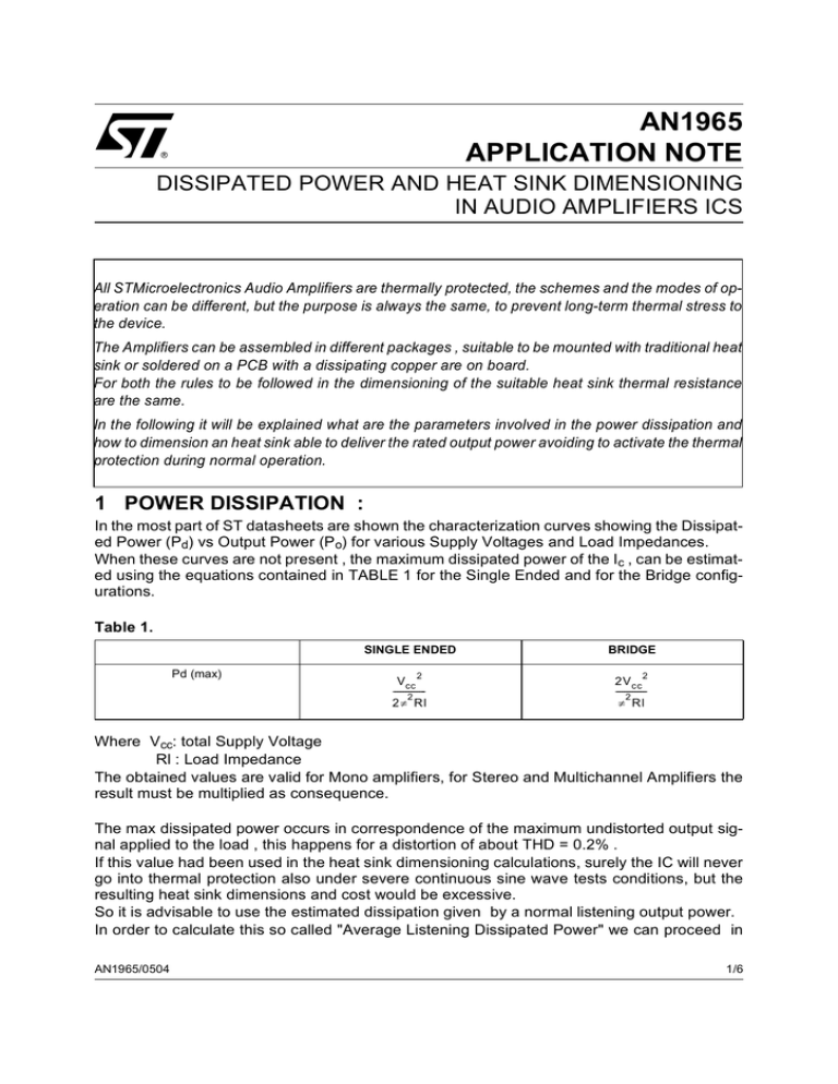
In the most part of ST datasheets are shown the characterization curves showing the Dissipated Power (Pd) vs Output Power (Po) for various Supply Voltages and Load Impedances.
When these curves are not present , the maximum dissipated power of the Ic , can be estimated using the equations contained in TABLE 1 for the Single Ended and for the Bridge configurations.
Table 1.
SINGLE ENDED
Pd (max)
2
Vcc
--------------2
2 π Rl
BRIDGE
2
2V c c
--------------2
π Rl
Where Vcc: total Supply Voltage
Rl : Load Impedance
The obtained values are valid for Mono amplifiers, for Stereo and Multichannel Amplifiers the
result must be multiplied as consequence.
The max dissipated power occurs in correspondence of the maximum undistorted output signal applied to the load , this happens for a distortion of about THD = 0.2% .
If this value had been used in the heat sink dimensioning calculations, surely the IC will never
go into thermal protection also under severe continuous sine wave tests conditions, but the
resulting heat sink dimensions and cost would be excessive.
So it is advisable to use the estimated dissipation given by a normal listening output power.
In order to calculate this so called "Average Listening Dissipated Power" we can proceed in
AN1965/0504
1/6
AN1965 APPLICATION NOTE
two different ways, that give similar results.
1.1 Gaussian Noise Test:
On the market are available test CD's containing Gaussian Noise traces that can be used to
define the Listening Dissipated Power.
You can proceed as follows:
– Apply the Gaussian Noise signal to the Amplifier input terminals, regulating the level in
such a way that the max Audio Signal Peaks observed with an Oscilloscope placed across
the load start to clip.
– With an Audio Analyzer measure the average Pout. In this conditions measure the Vcc and
Icc (Pin) and making the difference is obtained the Listening Average Dissipated Power.
As approximation the measured value it will be about a 40% less respect the Maximum Dissipated Power calculated with the equations in Table 1.
1.2 Theoretical Calculation:
Using as Audio source a typical CD music, normally the user will regulate the level in such a
way to listen the loudest part of the musical program without distortion.
Considering as maximum listening level a signal at THD = 0.5% (loudest part), it will come out
that the average listening level will be at about 12dB below (factor 15.85).
So using the Dissipation and the THD vs Pout Curves shown in the Datasheet it will be simple
to evaluate the Listening Average Dissipated Power.
P out ( THD = 0.5% )
P0av lis tening = --------------------------------------------------15.85
[1]
2 DETERMINING THE CORRECT HEAT SINK RTH:
In order to determine the suitable heat sink Rth, it's necessary to know a certain number of
quantities coming from the IC and the application characteristics:
a)
b)
c)
d)
e)
Average Listening dissipated power ( Pdav listening )
Max. ambient temperature ( Tamb )
Thermal Resistance Junction to case ( Rthj-c )
Max. Junction Temperature or Thermal Protection Threshold ( T j )
Thermal Resistance Case to Heat sink ( Rthc-s) due to the coupling medium.
The Average Listening dissipated power is calculated as shown in section 1.
The Maximum ambient temperature is dictated by the particular environment where the IC is
used, normally , for consumer Audio applications it ranges from 50°C < T amb(max)< 60°C.
The Thermal resistance Junction to case (Rthj-c) is specified in the datasheet and depends on
the used package and dissipating Silicon Area of the device.
The Thermal protection threshold is usually placed at a temperature close to Tj = 150°C, in
some device it could be different ( please refer to the interested datasheet ).
The thermal resistance due to the coupling medium placed between the IC case and the heat
sink (Rthc-s), can be 0.2°C/W in case of Thermal Grease or about 0.5°C/W if Silicon Rubber
washer is used .
2/6
AN1965 APPLICATION NOTE
Once the above mentioned parameters are known , the suitable heat sink thermal resistance
Rths-a can be easily calculated as follows:
T jmax – Tamb
Heat sin k R ths – a = ---------------------------------- – R thj – c – R th c – s
Pd lis tening
[2]
3 EXAMPLE 1:
Used device TDA7265 ( 25W + 25W Stereo Amplifier)
Applicative conditions:
Vcc
Rload
Rthj-c
Rthc-s
Tj max
Tamb max
=
=
=
=
=
=
+/-20V
2 x 8 ohm
2°C/W (max)
0.2°C/W used a thermal grease as thermal coupling medium
150°C
50°C
3.1 Maximum dissipated power (Pdmax):
The maximum dissipated power can be calculated via the curves shown in the datasheet
(fig.2) or with the equation in Table 1.
Pdmax = [ 402 / 2π2 8] = 10.1W for each channel
Pdmax = 20.2W for Stereo
From the fig.2 we can see that the measured Pdmax is about 19.5W so the two methods give
similar results both acceptable for the heat sink dimensioning.
If we use this value for the dimensioning we will obtain an heat sink not suitable for the real
applicative conditions in terms of cost and dimensions.
Figure 1. THD vs Pout
Figure 2. Pd vs Pout
3/6
AN1965 APPLICATION NOTE
As suggested in Section 2 it is advisable to use for the dimensioning the Average Listening
Dissipated Power [Pdav]. As mentioned in sec 2 we can obtain this value using two methods:
a) Gaussian Noise Test: with this approach we measured a value that is about 40% less respect
the Pdmax . The measured value is about 12W
b) Theoretical Value: (eq.1)
Poutav = Poutmax/ 15.85 = 25/ 15.85=1.58W (for each channel)
Looking at fig.2 this average output power gives a listening dissipated power of Pdav = 12W.
So using the two methods the result is the same.
Heat sink dimensioning:
from eq.[2] and using the values given in the applicative conditions it results
150 – 50
R ths – a = ---------------------- – 2 – 0.2 = 6.1 °C/W
12
This is the correct Rth value for the heat sink to be used in the application, if we want to take
in account some safety margin we can use an heat sink having an Rth of 5°C/W.
If the Pdmax have been used for the calculation the resulting heat sink Rth would be 2.8°C/W.
Note :
4/6
When a PowerDip or PSSO packages are used the procedure is identical , the only difference consists in dimensioning correctly
the Dissipating Copper Area on board.
In the datasheet are shown curves showing the Rthj-a vs Dissipating copper area.
AN1965 APPLICATION NOTE
Table 2. Revision History
Date
Revision
May 2004
1
Description of Changes
First Issue
5/6
AN1965 APPLICATION NOTE
The present note which is for guidance only, aims at providing customers with information regarding their products in
order for them to save time. As a result, STMicroelectronics shall not be held liable for any direct, indirect or
consequential damages with respect to any claims arising from the content of such a note and/or the use made by
customers of the information contained herein in connection with their products.
Information furnished is believed to be accurate and reliable. However, STMicroelectronics assumes no responsibility for the consequences
of use of such information nor for any infringement of patents or other rights of third parties which may result from its use. No license is granted
by implication or otherwise under any patent or patent rights of STMicroelectronics. Specifications mentioned in this publication are subject
to change without notice. This publication supersedes and replaces all information previously supplied. STMicroelectronics products are not
authorized for use as critical components in life support devices or systems without express written approval of STMicroelectronics.
The ST logo is a registered trademark of STMicroelectronics.
All other names are the property of their respective owners
© 2004 STMicroelectronics - All rights reserved
STMicroelectronics GROUP OF COMPANIES
Australia - Belgium - Brazil - Canada - China - Czech Republic - Finland - France - Germany - Hong Kong - India - Israel - Italy - Japan Malaysia - Malta - Morocco - Singapore - Spain - Sweden - Switzerland - United Kingdom - United States
www.st.com
6/6
