Self-Powered System with Wireless Data Transmission
advertisement
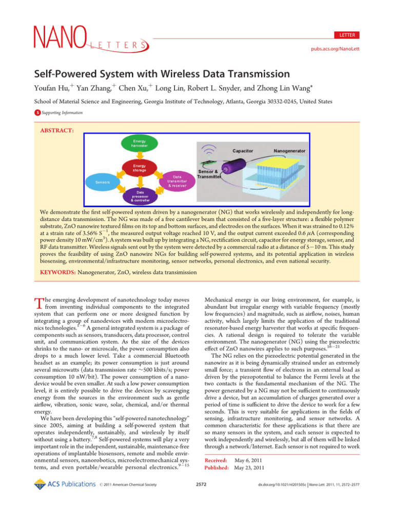
LETTER pubs.acs.org/NanoLett Self-Powered System with Wireless Data Transmission Youfan Hu,þ Yan Zhang,þ Chen Xu,þ Long Lin, Robert L. Snyder, and Zhong Lin Wang* School of Material Science and Engineering, Georgia Institute of Technology, Atlanta, Georgia 30332-0245, United States bS Supporting Information ABSTRACT: We demonstrate the first self-powered system driven by a nanogenerator (NG) that works wirelessly and independently for longdistance data transmission. The NG was made of a free cantilever beam that consisted of a five-layer structure: a flexible polymer substrate, ZnO nanowire textured films on its top and bottom surfaces, and electrodes on the surfaces. When it was strained to 0.12% at a strain rate of 3.56% S1, the measured output voltage reached 10 V, and the output current exceeded 0.6 μA (corresponding power density 10 mW/cm3). A system was built up by integrating a NG, rectification circuit, capacitor for energy storage, sensor, and RF data transmitter. Wireless signals sent out by the system were detected by a commercial radio at a distance of 510 m. This study proves the feasibility of using ZnO nanowire NGs for building self-powered systems, and its potential application in wireless biosensing, environmental/infrastructure monitoring, sensor networks, personal electronics, and even national security. KEYWORDS: Nanogenerator, ZnO, wireless data transimission T he emerging development of nanotechnology today moves from inventing individual components to the integrated system that can perform one or more designed function by integrating a group of nanodevices with modern microelectronics technologies.16 A general integrated system is a package of components such as sensors, transducers, data processor, control unit, and communication system. As the size of the devices shrinks to the nano- or microscale, the power consumption also drops to a much lower level. Take a commercial Bluetooth headset as an example; its power consumption is just around several microwatts (data transmission rate ∼500 kbits/s; power consumption 10 nW/bit). The power consumption of a nanodevice would be even smaller. At such a low power consumption level, it is entirely possible to drive the devices by scavenging energy from the sources in the environment such as gentle airflow, vibration, sonic wave, solar, chemical, and/or thermal energy. We have been developing this “self-powered nanotechnology” since 2005, aiming at building a self-powered system that operates independently, sustainably, and wirelessly by itself without using a battery.7,8 Self-powered systems will play a very important role in the independent, sustainable, maintenance-free operations of implantable biosensors, remote and mobile environmental sensors, nanorobotics, microelectromechanical systems, and even portable/wearable personal electronics.915 r 2011 American Chemical Society Mechanical energy in our living environment, for example, is abundant but irregular energy with variable frequency (mostly low frequencies) and magnitude, such as airflow, noises, human activity, which largely limits the application of the traditional resonator-based energy harvester that works at specific frequencies. A rational design is required to tolerate the variable environment. The nanogenerator (NG) using the piezoelectric effect of ZnO nanowires applies to such purposes.1621 The NG relies on the piezoelectric potential generated in the nanowire as it is being dynamically strained under an extremely small force; a transient flow of electrons in an external load as driven by the piezopotential to balance the Fermi levels at the two contacts is the fundamental mechanism of the NG. The power generated by a NG may not be sufficient to continuously drive a device, but an accumulation of charges generated over a period of time is sufficient to drive the device to work for a few seconds. This is very suitable for applications in the fields of sensing, infrastructure monitoring, and sensor networks. A common characteristic for these applications is that there are so many sensors in the system, and each sensor is expected to work independently and wirelessly, but all of them will be linked through a network/Internet. Each sensor is not required to work Received: May 6, 2011 Published: May 23, 2011 2572 dx.doi.org/10.1021/nl201505c | Nano Lett. 2011, 11, 2572–2577 Nano Letters Figure 1. Schematic diagram of the integrated self-powered system. (a) An integrated system can be divided into five modules: energy harvester, energy storage, sensors, data processor and controller, and data transmitter and receiver. (b) The prototype of an integrated self-powered system by using a nanogenerator as the energy harvester. continuously and simultaneously, instead, it will have a “blinking” working mode with a standby status and active status. The standby mode is normally longer, while the active mode is shorter. The energy scavenged and stored during the standby status can be used to drive it in the active mode. This means that these sensors periodically sample from their working environment and transmit data within a fraction of second. We can use the NG to harvest energy from the environment and store most of the energy when the sensor is in the standby mode. Then the collected energy will be used to trigger the sensor and then process and transmit the data in the active mode. An integrated self-powered system can be simply depicted in Figure 1a. The power source in this system includes the energy harvesting and storage modules. The harvester scavenges some kind of energy (solar, thermal, mechanical, and/or chemical) from the environment and stores it in the energy storage module. Thus the collected power is used to drive the other parts of the system. The sensors detect the changes in the environment, while the data processor and controller analyze the information. Then, the signal is sent out by the data transmitter, and simultaneously the response is received. In this paper, we demonstrate a prototype self-powered system that is made of an NG for harvesting mechanical energy, a low-loss full-wave bridge rectifier, a capacitor for storing the energy, an infrared photodetector, and a wireless data transmitter (as shown schematically in LETTER Figure 1b). The successful operation of this system is the first proof of utilizing a NG for a selfpowered wireless sensor networks. The NG used in the integrated system is a free-standing cantilever beam made of a five-layer structure using densely packed ZnO nanowire textured films. The NG was fabricated on a flexible polyester (PS) substrate (Dura-Lar, 220 μm in thickness), as shown in Figure 2a. First, a 5 nm thick Cr adhesion layer followed by a 50 nm thick ZnO seed layer were deposited at the selected rectangular region of 1 cm 1 cm on the top and bottom surfaces of the substrate. The ZnO seed layer is for growing densely packed ZnO nanowires via a wet chemical method.22,23 The nutrient solution we used in the chemical growth process of ZnO densely packed nanowires textured films was an equal molar aqueous solution of Zn(NO3)2 3 6H2O and hexamethylenetetramine (HMTA), and the concentration was 0.1 M. The nanowire films at the top and bottom surfaces were grown sequentially by placing the substrate at the top of the nutrient solution with one face down. Because of the surface tension, the substrate floated on the solution surface. Growth of ZnO nanowires was carried out in a mechanical convection oven (model Yamato DKN400, Santa Clara, CA) at 95 °C for 5 h. Figure 2b is a scanning electron microscope (SEM) image of the as-grown ZnO nanowires on the substrate. The dimensions of the nanowires were about 150 nm in diameter and 2 μm in length. From the cross section view, we can see that the ZnO nanowires were grown vertically from the substrate with a high packing density, and the bottoms of these nanowires were bonded through the ZnO seed layer. The insert of Figure 2b is the top view of the as-grown ZnO nanowires. Tweezers were used to scratch the top surfaces of these nanowires to establish that the top surfaces of these nanowires were also bonded together tightly in a uniform film (see Figure S1 in Supporting Information). Therefore, the entire ZnO structure could be regarded as a textured film24 that consisted of fully packed ZnO nanowire arrays between two parallel ZnO films. According to the growth mechanism,22 the c-axes for these nanowires were their growth direction, as shown in Figure 2a. Then, a thin layer of polymethyl methacrylate (PMMA) (MicroChem 950k A11) was spin coated on both surfaces of the substrate at the speed of 3000 rpm, followed by a Cr/Au layer deposition on the central rectangular area serving as the electrode of the NG. Finally, the whole device was fully packaged with polydimethylsiloxane (PDMS) to enhance the mechanical robustness and flexibility. The lower right corner of Figure 2a is a photo of a fabricated device. The size of the effective working area of the NG was 1 cm 1 cm. Two leads were connected to the top and bottom electrodes, respectively. It must be pointed out that the processing temperature was rather low (<100 °C) so that the entire process is adaptable for flexible electronics. We first calculated the distribution of piezopotential in the nanowire films in order to present its working mechanism. The entire structure of the NG was modeled as a cantilever beam with textured nanowire films on a common substrate. The films on the top and bottom surfaces had uniaxial texturing of [0001], respectively. We calculated the electric potential difference across the top and bottom electrodes when the entire structure was bent. Considering that the ZnO nanowire arrays grown on the substrate were close-packed with top and bottom ends bonded, they were represented by a thin film to simplify the calculation. The device was represented by a rectangular box with a dimension of 500 μm 500 μm 224 μm, as shown in Figure 2d. It is 2573 dx.doi.org/10.1021/nl201505c |Nano Lett. 2011, 11, 2572–2577 Nano Letters LETTER Figure 2. Nanogenerator fabrication and its working mechanism. (a) Fabrication process of the nanogenerator. The lower right parts are photos of a fabricated nanogenerator after packaging. The bending of the nanogenerator shows its good mechanical flexibility. (b) Cross section SEM image of the as-grown nanowire textured film on the substrate. The insert is the top view of the nanowire film. (d) The model for the simulation of the nanogenerator working mechanism. It was a triple-layer rectangular box, containing the flexible substrate and the ZnO films on the top and bottom surface. The calculated local potentials across the top electrode and bottom electrode are displayed in (c) and (e), respectively. (f) Distribution of the piezopotential in the designed structure if the ZnO NWs form a densily packed solid film that behaves like a continuous medium. The white dashed line in the substrate indicates the strain neutral plane. (g) Distribution of piezopotential in the designed structure if the ZnO NWs form a densily packed film but with a possibility of small gaps or interwire sliding, so that the NWs on the stretched side of the substrate may contribute nothing to the output voltage, while the NWs on the compressed side always create a piezopotential drop. a triple-layer structure, including two single crystal ZnO thin films (2 μm thick each) on the top and bottom surface of a polymer substrate (220 μm in thickness) (note the thickness of the electrodes were 100 nm, so they were ignored in the calculation). The material’s constants of ZnO used in the calculation are the same as in ref 25. The Young’s modulus, Poisson ratio, and the relative dielectric constants of the polymer substrate were E = 5 GPa, v = 0.33, and k = 3.2, respectively. All of the calculations were carried out by using the COMSOL package. The distribution of the piezoelectric potential was calculated by modeling the device structure as a cantilever beam with its one end being fixed (y = 0 plane in Figure 2d) and a transverse force being applied on its top edge at the other end (y = 500 μm plane in Figure 2d). The strain distribution in the cantilever was nonuniform. The mean strain in the beam applied in parallel to the substrate along the y-axis (see Figure 2d) was of 0.2%. To represent the metal electrodes in the NG, the top and bottom surfaces of the structure were set as equal potential planes, respectively, with the bottom one grounded. In the open circuit case, the total charge on the top and bottom surface must be zero. ZnO films were assumed to be intrinsic without doping. The piezoelectric potential has a large magnitude variation in the ZnO films. For easy visualization of the calculated potential, the local potential across the top (Figure 2c) and bottom (Figure 2e) electrodes of the NG under strain was present, also the potential inside the device is plotted in Figure 2d. From our calculation results, an 83.8 V inductive potential difference across the two electrodes was predicted. Such a potential drop across the top and bottom electrodes is the driving force for the transient flow of electrons in the external load. There are two scenarios if we consider the fact that the ZnO film is made of densely packed NWs. When the NG is bent, considering the neutral plane of strain is at the central of the substrate, as indicated by white dashed line in Figure 2f, the NW film on the stretched surface of the substrate is subject to a tensile stress, while the one on the compressed surface is under compressive stress. First, if the bonding between the NWs is very strong to form a solid film with considering that the growth direction of the NWs is along c-axis (polar direction for ZnO), a tensile stress perpendicular to the NWs results in a compressive strain along the c-axis direction, thus creating a piezopotential drop from the roots of the NWs to their top-ends, as shown in Figure 2f. At the same time, a corresponding compressive stress is applied to the NWs on the bottom surface of the substrate, resulting in a tensile strain along the c-axis, thus the top-ends of the NWs have a higher piezopotential than their roots. Therefore, the piezopotential drops in the top and bottom ZnO films have the same polarity, and they add up constructively. This piezopotential distribution will introduce induced charges in the top and bottom electrodes, and consequently generating the output voltage. Second, in a case that the bonding between the NWs is very weak with the possibility of interwire sliding/gaps, no piezoelectric potential would be produced by the film on the top surface of the substrate that is under tensile stress. But, considering the NWs are fully packed and can be squeezed between each other, a piezopotential drop is still created with some degradation 2574 dx.doi.org/10.1021/nl201505c |Nano Lett. 2011, 11, 2572–2577 Nano Letters LETTER Figure 3. Performance of a nanogenerator and design of an integrated system. (a) Output voltage and (b) output current of a typical nanogenerator. The voltage reached 10 V and the current exceeded 0.6 μA. (c) Schematic diagram of the designed self-powered system. For the wireless transmitter part, a phototransistor was used as the sensor to detect the light from an LED. The signal detected by the sensor was transmitted wirelessly by a single transistor RF transmitter. by the film at the substrate bottom surface that is subject to a compressive stress (see Figure 2g). Therefore, a potential drop is also expected between the top and bottom electrodes, but with its magnitude drops less than half in comparison to that in the first case. The actual bonding condition among nanowires should be between the two cases discussed above. Also, it is known that the as-grown ZnO nanowires have n-type doping, which can significantly screen the higher piezopotenital side, but leave the lower piezopotential side almost unchanged.26 Thus, the observed output voltage of the NG will be smaller than the theoretically calculated value due to the reasons list above. In practical measurements, a transverse mechanical triggering force was applied on the edge of the structure. When it was strained to 0.12% at a strain rate of 3.56% S1, the measured output voltage reached 10 V, and the output current exceeded 0.6 μA (corresponding volume current density 1 mA/cm3 and power density 10 mW/cm3), as shown in Figure 3a,b. The observed voltage is significantly smaller than the theoretically calculated value. Storage of the harvested energy was achieved by using an integrated low-loss full-wave bridge rectifier connected between the NG and a capacitor (Type 1210, 22 μF ( 10%, AVX). The entire integrated system was shown schematically in Figure 3c. To prove the possibility of wireless data transmission, we used a single transistor radio frequency (RF) transmitter to send out the detected electric signal. The oscillation frequency was tuned to be around 90 MHz, and a commercial portable AM/FM radio (CX-39, Coby) was used to receive the transmitted signal. First, we only tested the transmitting part of the circuit. When the transmitter was triggered by the stored energy harvested by the NG, there was a disturbing noise received by the radio (view the video in the Supporting Information). Because of the low power consumption (<1 mW) of the transmitter, the energy generated and stored during three straining cycles of the NG was enough to transmit the signal. The maximum transmission distance for our setup was over 5 m as limited by the quality of the receiver. Then a phototransistor in a slotted optical switch (OPB 825, OPTEK Technology) was added to the system as the photon detecting sensor to demonstrate that the self-powered system can work independently and wirelessly. The optical switch consisted of an infrared light-emitting diode (LED) and a NPN silicon phototransistor mounted in a low-cost black plastic housing on opposite sides of a 4 mm wide slot. The LED was triggered by a synthesized function generator (DS345, Stanford Research System) with a programmed voltage sequence to work as an external input light source, shining onto the phototransistor. The signal of the photocurrent generated by the phototransistor was periodically sent out using the energy stored in the capacitor. Because of the larger power consumption of the phototransistor (100 mW), it required the energy harvested for 1000 strain cycles of the NG (the performance of this NG was shown in Figure 4a) to simultaneously power the phototransistor and the transmitter (note that the driving time was 2025 ms). Each time when it was triggered, the signal received by the phototransistor modulated the transmitting signal, the information was received by the radio, and the demodulated signal was recorded from the headphone jack. The voltage sequence used to trigger the LED is shown in Figure 4b. Each cycle included an on (16 ms)/off (5 ms)/on (5 ms)/off (10 ms) status sequence. Figure 4c is the signal demodulated by the radio. The radio was tuned to work at a frequency avoiding the commercial radio signals around 90 MHz. When the phototransistor and the transmitter were triggered, there was a pulse detected beyond the noise background. If we enlarged this pulse, it contained a segment of the information that had the same waveform envelope as the triggering voltage sequence of the LED, as shown in Figure 4d in comparing with Figure 4c. This indicates that the wireless data transmission have been achieved by using this selfpowered system. 2575 dx.doi.org/10.1021/nl201505c |Nano Lett. 2011, 11, 2572–2577 Nano Letters LETTER Figure 4. Wireless data transmission. (a) Performance of the nanogenerator used in our wireless data transmission test. (b) The voltage sequence used to trigger the LED, which represented waveform envelope of the input signal. (c) Recorded signal from the headphone jack of the radio, which is detected and transmitted by our integrated self-powered system. (d) Enlargement of the pulse in (c). It shows a segment with the same waveform envelope as the initial excitation input signal. The red dashed lines show the corresponding time sequence in (b) and (d). For our NG structure, there are three factors that are important to the power output performance: the length of the nanowires, the thickness of the substrate, and the magnitude of the NG distortion. From the practical point of view, there are two modes to trigger the NG depending on the form of the mechanical energy scavenged by the NGs in the environment. For cases where the NGs are triggered at a constant stress, such as air flow, the calculated results show that the piezopotential between the two electrodes increases as the length of the nanowires is increased or the thickness of the substrate is decreased (see Figure S2 in Supporting Information). When the applied strain is fixed, such as when the NG is driven by the vibrations of a bridge where the trigger source is rigid, the piezopotential changes in the opposite sense compared to the former case. Thus, by adjusting the two competing factors, the thickness of the substrate and the length of the nanowire arrays, the device can be optimized to maximize its power harvesting efficiency to specific working situations according to the character of the scavenged energy in the environment. Increasing strain can also significantly enhance the output voltage (Figure S3 in Supporting Information). In addition, ZnO is a biocompatible and environmentally friendly material. The nanowire films can be grown at very low temperature (<100 °C) on any kind of substrate and any shape of substrate. These merits are critical for its industrial applications in flexible/ stretchable electronics and many areas. In conclusion, utilizing densely grown ZnO nanowire textured films grown on a polymer substrate by low-temperature chemical method has been demonstrated as an effective approach for harvesting low-frequency mechanical energy. An NG with a free cantilever beam construction was fabricated that was made of a five-layer structure: a flexible polymer substrate, ZnO nanowire textured films on its top and bottom surfaces, and electrodes on the surfaces. When it was strained to 0.12% at a strain rate of 3.56% S1, the measured output voltage reached 10 V, and the output current exceeded 0.6 μA for an NG that was 1 cm2 in size (corresponding power density 10 mW/cm3). By storing the energy generated by the NG, we have demonstrated a self-powered system that can work independently and wirelessly. The system was composed of an NG, rectification circuit, and capacitor for energy storage, sensor, and RF data transmitter. Wireless signals sent out by the system were detected by a commercial radio at a distance of 510 m. This study proves the feasibility of using ZnO nanowire NGs for building self-powered systems with capability of long distance data transmission, clearly proving its potential application in wireless biosensing, environmental infrastructure monitoring, sensor networks, personal electronics, and even national security. ’ ASSOCIATED CONTENT bS Supporting Information. Additional figures showing the nanowires grow vertically and finally join together to form a film by a cross-section TEM image, calculated piezopotential between the top and bottom electrodes as a function of the thickness of the substrate, performance characterization of the NG with increasing strain, and a video of testing the RF transmitter. This material is available free of charge via the Internet at http://pubs.acs.org. ’ AUTHOR INFORMATION Corresponding Author *E-mail: zlwang@gatech.edu. Author Contributions þ These authors contributed equally to this work. ’ ACKNOWLEDGMENT Research was supported by DARPA (HR0011-09-C0142, Program manager, Dr. Daniel Wattendorf), BES DOE 2576 dx.doi.org/10.1021/nl201505c |Nano Lett. 2011, 11, 2572–2577 Nano Letters LETTER (DE-FG02-07ER46394). Thanks to Dr. Yong Ding for help with TEM. ’ REFERENCES (1) Yu, G.; Lieber, C. M. Pure Appl. Chem. 2010, 82, 2295. (2) Avouris, P.; Martel, R. MRS Bull. 2010, 35, 306. (3) Dionne, J. A.; Sweatlock, L. A.; Sheldon, M. T.; Alivisatos, A. P.; Atwater, H. A. IEEE J. Sel. Top. Quantum Electron. 2010, 16, 295. (4) Lu, J.-Q. Proc. IEEE 2009, 97, 18. (5) Urban, G. A. Meas. Sci. Technol. 2009, 20, 012001. (6) Bogue, R. Sens. Rev. 2009, 29, 194. (7) Wang, Z. L.; Song, J. H. Science 2006, 312, 242. (8) Wang, Z. L. Sci. Am. 2008, 298, 82. (9) Glynne-Jones, P.; White, N. M. Sensor Rev. 2001, 21, 91. (10) Katz, E.; B€uckmann, A. F.; Willner, I. J. Am. Chem. Soc. 2001, 123, 10752. (11) Goldfarb, M.; Barth, E. J.; Gogola, M. A.; Wehrmeyer, J. A. IEEE/ASME Trans. Mechatronics 2003, 8, 254. (12) James, E. P.; Tudor, M. J.; Beeby, S. P.; Harris, N. R.; GlynneJones, P.; Ross, J. N.; White, N. M. Sens. Actuators, A 2004, 110, 171. (13) Beeby, S. P.; Tudor, M. J.; White, N. M. Meas. Sci. Technol. 2006, 17, R175. (14) Dondi, D.; Bertacchini, A.; Brunelli, D.; Larcher, L.; Benini, L. IEEE Trans. Ind. Electron. 2008, 55, 2759. (15) Owen, T. H.; Kestermann, S.; Torah, R.; Beeby, S. P. Sens. Rev. 2009, 29, 38. (16) Wang, X. D.; Song, J. H.; Liu, J.; Wang, Z. L. Science 2007, 316, 102. (17) Qin, Y.; Wang, X. D.; Wang, Z. L. Nature 2008, 451, 809. (18) Choi, M.-Y.; Choi, D.; Jin, M.-J.; Kim, I.; Kim, S.-H.; Choi, J.-Y.; Lee, S. Y.; Kim, J. M.; Kim, S.-W. Adv. Mater. 2009, 21, 2185. (19) Choi, D.; Choi, M.-Y.; Choi, W. M.; Shin, H.-J.; Park, H.-K.; Seo, J.-S.; Park, J.; Yoon, S.-M.; Chae, S. J.; Lee, Y. H.; Kim, S.-W.; Choi, J.-Y.; Lee, S. Y.; Kim, J. M. Adv. Mater. 2010, 22, 2187. (20) Xu, S.; Qin, Y.; Xu, C.; Wei, Y. G.; Yang, R. S.; Wang, Z. L. Nat. Nanotechnol. 2010, 5, 366. (21) Hu, Y. F.; Zhang, Y.; Xu, C.; Zhu, G.; Wang, Z. L. Nano Lett. 2010, 10, 5025. (22) Vayssieres, L. Adv. Mater. 2003, 15, 464. (23) Xu, S.; Lao, C. S.; Weintraub, B.; Wang, Z. L. J. Mater. Res. 2008, 23, 2072. (24) Hong, J.-I.; Bae, J.; Wang, Z. L.; Snyder, R. L. Nanotechnology 2009, 20, 085609. (25) Gao, Y. F.; Wang, Z. L. Nano Lett. 2007, 7, 2499. (26) Gao, Y. F.; Wang, Z. L. Nano Lett. 2009, 9, 1103. 2577 dx.doi.org/10.1021/nl201505c |Nano Lett. 2011, 11, 2572–2577
