Dec 2002 2500V/µs Slew Rate Op Amps Process Large Signals with
advertisement

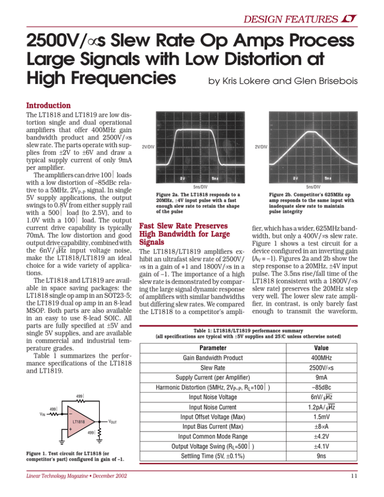
DESIGN FEATURES 2500V/µs Slew Rate Op Amps Process Large Signals with Low Distortion at High Frequencies by Kris Lokere and Glen Brisebois Introduction The LT1818 and LT1819 are low distortion single and dual operational amplifiers that offer 400MHz gain bandwidth product and 2500V/µs slew rate. The parts operate with supplies from ±2V to ±6V and draw a typical supply current of only 9mA per amplifier. The amplifiers can drive 100Ω loads with a low distortion of –85dBc relative to a 5MHz, 2VP–P signal. In single 5V supply applications, the output swings to 0.8V from either supply rail with a 500Ω load (to 2.5V), and to 1.0V with a 100Ω load. The output current drive capability is typically 70mA. The low distortion and good output drive capability, combined with the 6nV/√Hz input voltage noise, make the LT1818/LT1819 an ideal choice for a wide variety of applications. The LT1818 and LT1819 are available in space saving packages: the LT1818 single op amp in an SOT23-5; the LT1819 dual op amp in an 8-lead MSOP. Both parts are also available in an easy to use 8-lead SOIC. All parts are fully specified at ±5V and single 5V supplies, and are available in commercial and industrial temperature grades. Table 1 summarizes the performance specifications of the LT1818 and LT1819. 499Ω – 499Ω VIN VOUT LT1818 499Ω + Figure 1. Test circuit for LT1818 (or competitor’s part) configured in gain of –1. Linear Technology Magazine • December 2002 2V/DIV 2V/DIV 5ns/DIV 5ns/DIV Figure 2a. The LT1818 responds to a 20MHz, ±4V input pulse with a fast enough slew rate to retain the shape of the pulse Fast Slew Rate Preserves High Bandwidth for Large Signals The LT1818/LT1819 amplifiers exhibit an ultrafast slew rate of 2500V/ µs in a gain of +1 and 1800V/µs in a gain of –1. The importance of a high slew rate is demonstrated by comparing the large signal dynamic response of amplifiers with similar bandwidths but differing slew rates. We compared the LT1818 to a competitor’s ampli- Figure 2b. Competitor’s 625MHz op amp responds to the same input with inadequate slew rate to maintain pulse integrity fier, which has a wider, 625MHz bandwidth, but only a 400V/µs slew rate. Figure 1 shows a test circuit for a device configured in an inverting gain (AV = –1). Figures 2a and 2b show the step response to a 20MHz, ±4V input pulse. The 3.5ns rise/fall time of the LT1818 (consistent with a 1800V/µs slew rate) preserves the 20MHz step very well. The lower slew rate amplifier, in contrast, is only barely fast enough to transmit the waveform, Table 1: LT1818/LT1819 performance summary (all specifications are typical with ±5V supplies and 25°C unless otherwise noted) Parameter Value Gain Bandwidth Product 400MHz Slew Rate 2500V/µs Supply Current (per Amplifier) 9mA Harmonic Distortion (5MHz, 2VP–P, RL=100Ω) –85dBc Input Noise Voltage 6nV/√Hz Input Noise Current 1.2pA /√Hz Input Offset Voltage (Max) 1.5mV Input Bias Current (Max) ±8µA Input Common Mode Range ±4.2V Output Voltage Swing (RL=500Ω) ±4.1V Settling Time (5V, ±0.1%) 9ns 11 DESIGN FEATURES Low Distortion ADC Driver 1V/DIV 1V/DIV 5ns/DIV 5ns/DIV Figure 3a. LT1818 response to 50MHz, 4VP–P sine wave maintains good fidelity. turning it into a triangle wave. The difference in slew rate also has important ramifications for distortion of sine waves. Figures 3a and 3b show the response of both amplifiers to a 50MHz, 4VP–P sine wave. The LT1818 transmits the waveform with minimal distortion, but the competitor’s part turns the sine wave into a triangle wave, a result of the lower slew rate. This demonstrates that, to accurately process real world signals, slew rate is often the limiting parameter rather than bandwidth. + VIN + 1/2 LT1819 – 1/2 LT1819 – 432Ω 432Ω 200Ω 200Ω 3pF Figure 4. Dual op amp cascaded to form a gain of 10 (20dB). VOUT Figure 3b. Competitor’s 625MHz response to the same sine wave is distorted. The application shown in Figure 4 demonstrates the excellent high-frequency response of the LT1819 dual amplifier, and how two op amps can be combined to further increase bandwidth. The circuit shows the dual LT1819 op amp configured as two cascaded gain stages that together form a gain of 10 (= 20dB). The feedback capacitor on the second stage serves to cancel a pole formed by the feedback resistors and the input capacitance, to reduce peaking and ringing. The frequency-domain response (Figure 5) shows the –3dB frequency at 80MHz, which represents a gain-bandwidth product of 800MHz, consistent with two 400MHz amplifiers in series. Figure 6 shows the transient response to a small step. The 3.5ns rise/fall time is consistent with an 80MHz –3dB bandwidth. Figure 7 shows that the step response is only a little slower making a transition to a full 6VP–P, showing the merits of a high slew rate. Figure 8 illustrates the use of the LT1818 as a buffer for the LTC1744 14-Bit 50Msps ADC. The amplifier must provide low noise, low distortion as well as fast settling characteristics in order to recover quickly from the sampling loading effects of the ADC. The LTC1744 signal-to-noise ratio (SNR) of 73.5dB at 2VP–P implies an input referred noise of 149µVRMS. The 6nV/√Hz input voltage noise of the LT1818, integrated over a 94MHz bandwidth (formed by the 51.1Ω, 18pF and the CIN of the ADC) results in only 91µVRMS of input noise. The contribution of the input referred current noise of the LT1818 depends on the source resistance of the circuit that drives the LT1818. For a 1k source resistance, the 1.2pA/√Hz input current noise results in 18µVRMS over the same bandwidth. Both noise sources taken together still do not degrade the noise performance of the 14-bit ADC. Figure 9 shows the 4096 bin FFT of the converter output. This implies a full scale SNR of 76dB, just slightly better than the ADC’s typical 73.5dB specification. More readily seen in the FFT is the SFDR of 78dB. You can further improve the performance of the circuit by using the two amplifiers of the LT1819 to convert the single-ended input signal to a differential signal and drive both inputs of the LTC1744, as shown in Figure 10. An advantage of driving the ADC differentially is that the signal swing at each input can be reduced, which reduces the distortion of both the ADC and the amplifier. Typical performance is shown in the 25 20 GAIN (dB) 15 10 5 20mV/ DIV 1V/DIV 0 –5 VS = ±5V TA = 25°C –10 100k 1M 10M FREQUENCY (Hz) 100M Figure 5. Frequency-domain response of 20dB gain block 12 10ns/DIV Figure 6. Small-signal transient response of 20dB gain block 10ns/DIV Figure 7. Large-signal transient response of 20dB gain block Linear Technology Magazine • December 2002 DESIGN FEATURES 0 –20 + 51.1Ω AIN+ LT1818 – 18pF 2.5V AIN– –30 LTC1744 14 BITS 50Msps (SET FOR 2VP-P FULL SCALE) AMPLITUDE (dBc) 2.5VDC ±1VAC fIN = 5.102539MHz fS = 50Msps VIN = 300mVP-P SFDR = 78dB 8192 SAMPLES NO WINDOWING OR AVERAGING –10 5V 5V –40 –50 –60 –70 2 3 –80 –90 Figure 8. Single ended ADC driver –100 –110 VIN ±0.5VAC 18pF + 5M 0 + 18pF 536Ω AIN– 4.99k –20 –30 51.1Ω 1/2 LT1819 + fIN = 5.023193MHz fS = 50Msps VIN = 750mVP-P SFDR = 81dB 8192 SAMPLES NO WINDOWING NO AVERAGING –10 LTC1744 14 BITS 50Msps (SET FOR 2VP-P FULL SCALE) AMPLITUDE (dBc) AIN – 25M 5V – 536Ω 10M 15M 20M FREQUENCY (Hz) Figure 9. FFT of single ended ADC driver 51.1Ω 1/2 LT1819 5V 0 5V 10µF 18pF –40 –50 –60 –70 –80 –90 –100 4.99k –110 0.1µF –120 0 Fast Edge Generation to Measure Slew Rate A 2500V/µs slew rate implies that the transition between ±2V occurs in 1.6ns. In order to accurately measure slew rates this fast, it is necessary to generate an input step that is faster than the device-under-test. Many offthe-shelf function generators fail in this regard, in which case custommade circuitry may be necessary. The widely used HP8110A 100MHz Pulse Generator, for example, has a minimum rise/fall time of 1.8ns, which fails to provide a fast enough stimu- 10M 15M 20M FREQUENCY (Hz) 25M Figure 11. FFT of single-todifferential ADC driver Figure 10. Single-to-differential ADC driver FFT of Figure 11, again consisting of 4096 bins derived from 8192 samples. 5M lus for this test. The older HP8082A Pulse Generator provides 1ns transitions, but its output amplitude is only 5V into 50Ω, which limits its flexibility to drive the amplifier on ±5V supplies. The simple circuit of Figure 12 uses a high-speed inverter such as the NC7SZU04. Since the inverter has high gain, it sharpens the input edge of whatever pulse generator is used to drive it. The output is AC coupled to level shift the single sup- ply inverter output to drive a split supply biased op amp. This inverter can provide rise and fall times as fast as 0.8ns, but the maximum supply voltage (and hence the maximum swing) is 5.5V, which is just short of the ±3V or ±4V desired for full range slew rate testing of the LT1818/ LT1819. In addition, the 16mA output current drive of the inverter precludes a 50Ω termination, which limits the universal applicability of this circuit. +V1 750Ω D1 750Ω D2 15V 5.5V – VIN VOUT D3 D4 750Ω Figure 12. A simple inverter used to generate a sharp pulse—fast but too little signal swing and output drive Linear Technology Magazine • December 2002 ±V1 = ±14V –V1 51Ω 1µF 1µF VOUT LT1210 + VIN D5 D6 –15V –V2 +V2 D1–D4: IN5711 D5, D6: METELICS MMD-0840 (408) 737-8181 Figure 13. Improved pulse-sharpener circuit 13 DESIGN FEATURES 1V/DIV 500ps/DIV Figure 14. Output of pulse-sharpener circuit Figure 13 shows a more involved, but very flexible and fast solution. The diode bridge D1-D4 switches the LT1210 current-feedback amplifier, which runs off ±15V supplies. This way, the input edge does not need to swing more than ±1V, and the current into the inverting node of the LT1210 switches very quickly. The already fast waveform at the output of the amplifier is then AC coupled into the D5–D6 Step Recovery Diodes (SRD). An SRD is a two terminal p-i-n junction whose DC characteristics are similar to the usual p-n junction diode, but whose switching characteristics are quite different. The most distinguishing feature of the SRD is the very abrupt dependence of its junction impedance upon its internal charge storage. If a forward biased SRD is suddenly reverse-current biased, it will first appear as a very low impedance until the stored charge is depleted. Then the impedance will suddenly increase to its normal high reverse value, thereby stopping the flow of reverse current. This impedance transition generally takes only a few hundred picoseconds. The circuit in Figure 13 uses this SRD property as a pulse sharpener, generating a sub-one-nanosecond edge at the output. You can set the voltage levels of the output waveform by adjusting ±V2. Figure 14 shows a 5V, 0.8ns output waveform generated by this circuit. Finally, an important consideration in these measurements is the bandwidth of the oscilloscope used. The photograph in Figure 14 is taken with a Tektronix TDS820 6GHz digitizing oscilloscope. For a detailed description of the effect of slower oscilloscopes on measuring fast edges, refer to Linear Technology Application Note 47. LT1818 Circuit Design A simplified schematic of the LT1818/ LT1819 is shown in Figure 15. Both inputs are high impedance, classifying the amplifier as a voltage feedback topology. Complementary NPN and PNP emitter followers Q1-Q8 buffer each input and present the differential input signal across the internal resistor R1. The input common mode range extends to typically 0.8V from either supply, and is limited by a VBE of Q10/Q14 plus a VSAT of Q5/Q6. NPN and PNP current mirrors Q10– Q11 and Q14–Q15 mirror the current generated through R1 into the high impedance node. Cascode devices Q9 and Q13 raise the output impedance of the mirror, improving the open loop gain. Resistor R1, the transconductances of Q5–Q8, and the compensation capacitor C1 set the 400MHz gain bandwidth product of the amplifier. The RC, CC network between the high impedance node and the output provides extra compensation when the output drives a capacitive load. This keeps the LT1818/LT1819 unity-gain stable with a CLOAD up to 20pF. The amplifier can drive larger capacitive loads when configured in higher noise gains, or with an isolation resistor of 10Ω to 50 Ω in series with the load. The R2, C2 networks on the current mirrors provide a pole and zero at a frequency below the unity-gain frequency. This lowers the frequency where the open loop gain crosses 0dB, which improves the phase margin of the amplifier while maintaining a high open loop gain at lower frequencies. The current generated across R1, divided by the capacitor C1, determines the slew rate. Note that this current, and hence the slew rate, are proportional to the magnitude of the input step. The input step equals the output step divided by the closed loop gain. The highest slew rates are there- V+ C2 Q11 Q27 Q10 Q12 Q26 Q25 Q24 R2 Q19 Q9 Q17 RC Q3 – IN CC Q5 Q7 OUT R1 Q2 Q4 Q8 Q1 +IN Q18 Q20 Q13 R2 Q28 C2 Q21 C1 Q6 Q14 Q15 Q16 Q22 Q23 V– Figure 15. Simplified schematic of LT1818/LT1819 amplifier 14 Linear Technology Magazine • December 2002 DESIGN FEATURES fore obtained in the lowest gain configurations. The 2500V/µs slew rate specified on the data sheet is measured in a noninverting unity gain configuration. The 1800V/µs production tested slew rate is measured in an (inverting) gain of –1, which is equivalent to a noninverting gain of 2. The internal current generated across the input resistor can be much higher than the quiescent supply current (up to 80mA). In normal transient closed loop operation this does not present a problem, since after a few nanoseconds the feedback brings the differential input signal back to zero. However, sustained (i.e. open loop) differential input voltages may result in excessive power dissipation and therefore this amplifier should not be used as a comparator. The output stage buffers the high impedance node from the load by providing current gain. Emitter followers Q17–Q20 provide a current gain equal to BetaNPN × BetaPNP, but the effective current gain is greatly enhanced by the dynamic base current compensation provided by Q24–Q26 and Q21–Q23. Q24 measures a fraction of the output current that flows through Q19, and mirror Q25–Q26 injects the appropriate current back into the base of Q19. This signal-dependent boost improves the linearity of the amplifier by reducing the amount of differential input signal required for a given output current. An additional advantage is that the output devices can be smaller, which requires less quiescent current for a given amplifier speed. LTC4412, continued from page 4 High Side Power Switch voltage, therefore denying power to the load. The MOSFET is connected with its source connected to the power source. This prevents the drain-source diode from supplying voltage to the load when the MOSFET is off. no load current is drawn from the batteries. The STAT pins provide information as to which input is supplying the load current. This concept can be applied to as many power inputs as are needed. Multiple Battery Charging Figure 6 shows an application circuit for automatically charging two batteries from a single charger. Whichever battery has the lower voltage receives the charging current until both battery voltages are equal then both will be charged. When both are charged simultaneously the higher capacity battery receives proportionally higher current from the charger. For Li-Ion batteries both batteries achieve the float voltage of the battery charger minus the forward regulation voltage of 20mV. This concept can apply to more than two batteries. The STAT pins provide information as to which batteries are being charged. Figure 7 illustrates an application circuit for a logic controlled high side power switch using the control input pin. When the CTL pin is a logical low the LTC4412 turns on the MOSFET. Because the SENSE pin is grounded the LTC4412’s internal controller functions as an open-loop comparator and applies maximum gate drive voltage to the MOSFET. When the CTL pin is a logical high the LTC4412 turns off the MOSFET by pulling its gate voltage up to the supply input Q1 * SUPPLY INPUT LOGIC INPUT TO LOAD LTC4412 6 1 VIN SENSE 5 2 GND GATE 4 3 CTL STAT COUT Conclusion The ultrafast slew rate and high bandwidth allow the LT1818 and LT1819 op amps to process large signals at high frequencies with low distortion. Combined with the low noise and moderate supply current, these amplifiers are a good choice for receivers, filters, or drivers of cables and ADCs in high-speed communication or data acquisition systems. Conclusion The LTC4412 provides a simple and efficient way to implement a low loss ideal diode controller that extends battery life and significantly reduces self-heating. The low external parts count translates directly to low overall system cost and its ThinSOT 6-pin package makes for compact design solutions. It’s versatile enough to be used in a variety of diode OR-ing applications covering a wide range of supply voltages. 4412 F07 *PARASITIC DRAIN-SOURCE DIODE OF MOSFET Q1: FAIRCHILD SEMICONDUCTOR FDN306P (408) 822-2126 Figure 7. Logic controlled high side power switch for the latest information on LTC products, visit www.linear.com Linear Technology Magazine • December 2002 15


![5: “OPERATIONAL AMPLIFIER IMPERFECTIONS AND APPLICATIONS” [1, pg. 23]](http://s2.studylib.net/store/data/014264266_1-2db71c70e14bfbbd5962c9add234b539-300x300.png)


