UNIVERSITY OF OSLO Faculty of mathematics and natural sciences
advertisement
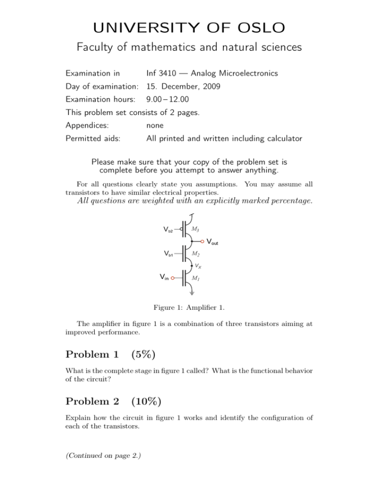
UNIVERSITY OF OSLO Faculty of mathematics and natural sciences Examination in Inf 3410 — Analog Microelectronics Day of examination: 15. December, 2009 Examination hours: 9.00 – 12.00 This problem set consists of 2 pages. Appendices: none Permitted aids: All printed and written including calculator Please make sure that your copy of the problem set is complete before you attempt to answer anything. For all questions clearly state you assumptions. You may assume all transistors to have similar electrical properties. All questions are weighted with an explicitly marked percentage. Vb2 M3 Vout Vb1 M2 VX Vin M1 Figure 1: Amplifier 1. The amplifier in figure 1 is a combination of three transistors aiming at improved performance. Problem 1 (5%) What is the complete stage in figure 1 called? What is the functional behavior of the circuit? Problem 2 (10%) Explain how the circuit in figure 1 works and identify the configuration of each of the transistors. (Continued on page 2.) Examination in Inf 3410, 15. December, 2009 Problem 3 Page 2 (20%) Determine the small signal voltage gain of the circuit in figure 1. Take the body effect into account. M3 Vout Vb M2 VX Vin M1 Figure 2: Amplifier 2. Problem 4 (25%) Determine the small signal voltage gain of the circuit in figure 2. Take the body effect into account. Problem 5 (10%) By comparing the voltage gain expressions, determine which of the two amplifiers has the highest gain. M3 Vb Vin Vout M2 CL VX M1 Figure 3: Amplifier 2 with load capacitor. Problem 6 (30%) Determine the frequency dependant transfer function, H(s), of the amplifier in figure 3. For simplicity we ignore all capacitances except for the output load capacitance.
