A 4.2 GHz PLL Frequency Synthesizer with an Adaptively Tuned
advertisement
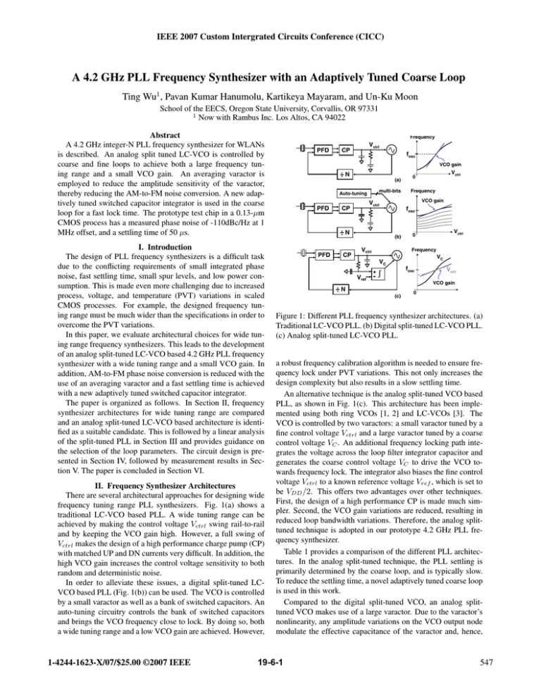
IEEE 2007 Custom Intergrated Circuits Conference (CICC) A 4.2 GHz PLL Frequency Synthesizer with an Adaptively Tuned Coarse Loop Ting Wu1 , Pavan Kumar Hanumolu, Kartikeya Mayaram, and Un-Ku Moon School of the EECS, Oregon State University, Corvallis, OR 97331 1 Now with Rambus Inc. Los Altos, CA 94022 Abstract A 4.2 GHz integer-N PLL frequency synthesizer for WLANs is described. An analog split tuned LC-VCO is controlled by coarse and fine loops to achieve both a large frequency tuning range and a small VCO gain. An averaging varactor is employed to reduce the amplitude sensitivity of the varactor, thereby reducing the AM-to-FM noise conversion. A new adaptively tuned switched capacitor integrator is used in the coarse loop for a fast lock time. The prototype test chip in a 0.13-µm CMOS process has a measured phase noise of -110dBc/Hz at 1 MHz offset, and a settling time of 50 µs. II. Frequency Synthesizer Architectures There are several architectural approaches for designing wide frequency tuning range PLL synthesizers. Fig. 1(a) shows a traditional LC-VCO based PLL. A wide tuning range can be achieved by making the control voltage Vctrl swing rail-to-rail and by keeping the VCO gain high. However, a full swing of Vctrl makes the design of a high performance charge pump (CP) with matched UP and DN currents very difficult. In addition, the high VCO gain increases the control voltage sensitivity to both random and deterministic noise. In order to alleviate these issues, a digital split-tuned LCVCO based PLL (Fig. 1(b)) can be used. The VCO is controlled by a small varactor as well as a bank of switched capacitors. An auto-tuning circuitry controls the bank of switched capacitors and brings the VCO frequency close to lock. By doing so, both a wide tuning range and a low VCO gain are achieved. However, 1-4244-1623-X/07/$25.00 ©2007 IEEE PFD CP fosc VCO gain N (a) multi-bits Auto-tuning PFD N PFD CP N Frequency fosc (b) Vctrl Vctrl 0 Frequency VC VC Vref Vctrl 0 VCO gain Vctrl CP + - fosc 1 I. Introduction The design of PLL frequency synthesizers is a difficult task due to the conflicting requirements of small integrated phase noise, fast settling time, small spur levels, and low power consumption. This is made even more challenging due to increased process, voltage, and temperature (PVT) variations in scaled CMOS processes. For example, the designed frequency tuning range must be much wider than the specifications in order to overcome the PVT variations. In this paper, we evaluate architectural choices for wide tuning range frequency synthesizers. This leads to the development of an analog split-tuned LC-VCO based 4.2 GHz PLL frequency synthesizer with a wide tuning range and a small VCO gain. In addition, AM-to-FM phase noise conversion is reduced with the use of an averaging varactor and a fast settling time is achieved with a new adaptively tuned switched capacitor integrator. The paper is organized as follows. In Section II, frequency synthesizer architectures for wide tuning range are compared and an analog split-tuned LC-VCO based architecture is identified as a suitable candidate. This is followed by a linear analysis of the split-tuned PLL in Section III and provides guidance on the selection of the loop parameters. The circuit design is presented in Section IV, followed by measurement results in Section V. The paper is concluded in Section VI. Frequency Vctrl Vctrl VCO gain (c) 0 Figure 1: Different PLL frequency synthesizer architectures. (a) Traditional LC-VCO PLL. (b) Digital split-tuned LC-VCO PLL. (c) Analog split-tuned LC-VCO PLL. a robust frequency calibration algorithm is needed to ensure frequency lock under PVT variations. This not only increases the design complexity but also results in a slow settling time. An alternative technique is the analog split-tuned VCO based PLL, as shown in Fig. 1(c). This architecture has been implemented using both ring VCOs [1, 2] and LC-VCOs [3]. The VCO is controlled by two varactors: a small varactor tuned by a fine control voltage Vctrl and a large varactor tuned by a coarse control voltage VC . An additional frequency locking path integrates the voltage across the loop filter integrator capacitor and generates the coarse control voltage VC to drive the VCO towards frequency lock. The integrator also biases the fine control voltage Vctrl to a known reference voltage Vref , which is set to be VDD /2. This offers two advantages over other techniques. First, the design of a high performance CP is made much simpler. Second, the VCO gain variations are reduced, resulting in reduced loop bandwidth variations. Therefore, the analog splittuned technique is adopted in our prototype 4.2 GHz PLL frequency synthesizer. Table 1 provides a comparison of the different PLL architectures. In the analog split-tuned technique, the PLL settling is primarily determined by the coarse loop, and is typically slow. To reduce the settling time, a novel adaptively tuned coarse loop is used in this work. Compared to the digital split-tuned VCO, an analog splittuned VCO makes use of a large varactor. Due to the varactor’s nonlinearity, any amplitude variations on the VCO output node modulate the effective capacitance of the varactor and, hence, 19-6-1 547 ICP 2π θin(s) Table 1: Comparison of PLL frequency synthesizers. Architecture Traditional Digital split-tuned Analog split-tuned Tuning range VCO gain Vctrl swing PLL Settling large high extreme fast large low moderate slow large low fixed slow Varactor size VCO AM-FM big high small low big high K of s Cr R2 1 sR 3C3 C2 (a) |G(s)| ωe = the oscillation frequency. This mechanism, called amplitudemodulation (AM) to frequency-modulation (FM) noise conversion, is a significant source of VCO phase noise. It has been shown that [4], this noise is related to the amplitude sensitivity, ∆C/∆A, where ∆C is the change in the varactor capacitance due to a change in the VCO output voltage ∆A. To reduce the AM-FM noise conversion, an averaging varactor is employed in this work. The averaging varactor improves the varactor’s linearity and reduces the amplitude sensitivity, thereby lowering the VCO phase noise. (1) where ωc is approximately the loop bandwidth, and is given by (ICP R2 /2π) · (Kof /N ). The PLL overall loop gain GT (s) can be expressed as the sum of GF (s) and GC (s). ¿From (1), Koc ωz ω3 ωc ωr ωz + (1 + ) s s + ωr s Kof s2 (2) The bode plot of the loop gains are conceptually shown in Fig. 2(b). A point of interest is the frequency where the fine loop gain and coarse loop gain are equal. It can be shown that this frequency ωe is approximated by ωe = Koc ω3 Kof (3) In the overall loop gain GT (s), the coarse loop gain GC (s) is dominant at frequencies below ωe , and the fine loop gain GF (s) is dominant at frequencies larger than ωe . In order for the coarse loop to have a negligible impact on the PLL dynamic and stability, the frequency ωe should be lower than ωz . As a result, 1 Koc Koc 1 < ⇒ R3 C3 > R2 C2 Kof R3 C3 R2 C2 Kof (4) Eq. (4) illustrates a lower limit for the coarse loop parameters R3 C3 due to the loop stability constraint. On the other hand, GF(s) GC(s) 0 ωr ωe ωz ωc Log(ω) (b) Figure 2: (a) Linear model for the analog split-tuned VCO based PLL. (b) Bode plot of open loop gains. FF FED REF (fref) In (6fref) PFD UP DN CP ICP CLK GEN Φ1,Φ Φ2 P/S Cr R2 R4 Vctrl C4 VC VCO C3 C2 V2 Vref 4/5 SC + - OUT GF (s) ≈ K oc 1 K of R 3C3 2 III. Linear Analysis Fig. 2(a) shows the linear model for the analog split-tuned VCO based PLL, where Kof and Koc are the VCO gain for the fine and coarse control nodes, respectively. The fine loop has a 2nd -order loop filter with a zero frequency of ωz = R21C2 and a pole frequency of ωr = R21Cr . The coarse loop employs a first order integrator with a transfer function (1/sR3 C3 = ω3 /s). Assuming ωz ! ωr (C2 " Cr ), the fine loop gain GF (s) and the coarse loop gain GC (s) can be found to be GT (s) = K oc s 1/N GT(s) ωz ωr ωc (1 + ) s s s + ωr ωc ωz ω3 Koc ωr GC (s) ≈ s3 Kof s + ωr θo(s) Figure 3: The proposed analog split-tuned LC-VCO based PLL frequency synthesizer. during lock-in process, the charge-pump output voltage Vctrl would saturate to either the power or ground rail. The coarse loop aids the PLL frequency lock by slewing up or down the coarse control voltage VC to the desired value. Assume the PLL settling time is dominated by the settling time of the coarse control voltage. If the PLL is required to switch an output frequency from ωosc to (ωosc ± ∆ωosc ) within a time period of TS , then VDD Koc VDD TS TS Koc > ∆ωosc ⇒ R3 C3 < 2R3 C3 2 ∆ωosc (5) Eq. (5) yields an upper limit for R3 C3 . As a consequence, the design of the coarse control loop must trade off between the loop stability and settling time. To decouple this trade-off and to reduce the settling time, new techniques need to be developed. IV. Circuit Design A. Overall Architecture The proposed PLL frequency synthesizer depicted in Fig. 3 consists of a PFD, a CP, a 3rd -order loop filter, an analog splittuned LC-VCO, and a pulse-swallow counter. With a 16 MHz reference frequency and a division ratio between 256 to 263, this PLL synthesizer operates in the 4.2 GHz frequency range∗ . A switched-capacitor (SC) integrator is employed in the coarse ∗ RF in the 5 GHz WLAN 802.11a lower band can be achieved by mixing the VCO output and its divided-by-4 output [5]. 19-6-2 548 ~Tref /6 UP V2 S1 V2 CS Vref S2 S1 Φ3 DN S2 Vref (a) VDD ~Tref /6 Φ4 Mp0 Φ5 S1 CS S4 S5 2CS 2CS S3 2CS S2 7.0/0.5 Mp1 1.0nH IO 7.0/0.5 VF 7.0/0.5 V 2pF F 100/0.5 V100/0.5 2pF ctrl VC 2pF 4pF 4pF 140/0.5 VC 4K 4K 1.0nH Vctrl VC S1 V 4KC S2 (b) M1 1K M2 4K 1K V1 V2 V3 Figure 4: Switched-capacitor circuitry in the coarse loop. (a) Conventional design. (b) Proposed adaptively tuned design. 1.6 Effective varactor capacitance (pF) FED 5CS UP 3CS DN Fixed SC CS CS Φ3 T/8 Φ5 Φ1 Φ2 overlap with Φ1 and Φ2 3CS 3CS (a) 5CS Average SR for VC (10-3 V/µ µs) Φ4 T/4 (b) UP ⊕ DN T/2 Fixed SC Adaptively tuned SC 10 5 0 1.4 0.5 V =1.0 G VG=1.5 V =0.5 G Average Simulated ∆ C / ∆ A (pF/V) Sampling capacitance Adaptively tuned SC 7CS REF Sampling capacitance Figure 6: LC-VCO with an averaging varactor. 1.2 1 0.8 0.25 0 −0.25 0.6 V =1.0 G V =1.5 G V =0.5 G 2 -6 -4 -2 4 Average 6 0.4 0 0 0.5 1 Coarse control voltage V (V) C (a) 1.5 −0.5 0 0.5 1 1.5 Coarse control voltage VC (V) (b) -5 -10 Frequency difference between REF and FED (%) (c) Figure 5: (a) Timing diagram of the adaptively tuned SC integrator. (b) Effective sampling capacitance. (c) Comparison of the simulated slew rates for the coarse control voltage VC . loop. A clock generator produces the reference clock for the PLL. It also generates two non-overlapping clock phases, Φ1 and Φ2, with the same frequency as the reference for the SC integrator. The exclusive-OR (XOR) of UP and DN pulses from the PFD is also fed into the SC integrator. This will adaptively bring the PLL into lock, hence reducing the settling time. B. Adaptively Tuned SC Integrator Fig. 4(a) shows the conventional switched-capacitor circuitry with a sampling capacitance of CS . In this work as shown in Fig. 4(b), three additional sampling capacitors with capacitance values of 2CS are inserted and controlled by signals Φ3, Φ4, and Φ5, respectively. To generate Φ3, the PFD output UP and DN pulses are fed into an XOR gate. The pulses Φ4 and Φ5 are simply the delayed outputs of Φ3. The timing diagram is shown in Fig. 5(a). When the loop is in lock, the XOR output is zero. The additional sampling capacitors have no impact on the original SC integrator. When the loop is unlocked, an increased phase error between the reference and feedback clocks leads to an increased pulse width of the XOR output. If the XOR and its delayed outputs have an overlap with both phases Φ1 and Φ2, the additional sampling capacitors are effectively added in parallel with the original capacitor CS . As a result, the effective sampling capacitance is still CS when the loop is in lock, but it will become 3CS , 5CS , and 7CS when the XOR output pulse width is larger than 1/8, 1/4, and 1/2 of the reference clock period (Fig. 5(b)). The increased sampling capacitance will re- Figure 7: Comparisons of simulated (a) effective capacitance of varactor, (b) sensitivity of VCO output voltage. duce the time constant of the SC integrator, thereby improving the PLL settling behavior. Fig. 5(c) shows the simulated average slew rate (SR) for the coarse control voltage VC as a function of the frequency difference between the reference clock and the feedback clock. When the two frequencies are close, the adaptively tuned SC circuit behaves the same as the conventional SC circuit. When the two frequencies differ from each other, i.e., the loop is unlocked, the adaptively tuned SC integrator provides an increased slew rate for VC with an increased frequency difference. As a result, the settling time is reduced without any penalty in the loop stability. C. Split-Tuned VCO with an Averaging Varactor The split-tuned VCO with an averaging varactor is shown in Fig. 6. Two varactors are sized with a ratio of 20 and controlled by Vctrl and VC , respectively. For each varactor, three MOS varactors are connected in parallel with DC bias voltages V1 to V3 . Rather than using a fixed DC bias voltage (i.e., V1 = V2 = V3 ) as in the traditional varactor designs, the averaging varactor uses distributed voltage values for V1 to V3 . As a result, the nonlinearities of the three varactors are cancelled to a first order. Fig. 7(a) shows the simulated effective capacitance of the conventional varactor when the DC bias voltage VG is set to be 0.5, 1.0, and 1.5, respectively, compared to the capacitance of the averaging varactor. The averaging varactor also reduces the amplitude sensitivity, ∆C/∆A, as shown in Fig. 7(b). Simulation results also show that at 1 MHz offset, a 3 dB improvement in phase noise is achieved in the 4.2 GHz operating frequency range. Although this averaging varactor is similar to the varactor proposed in [6], the focus of this work is on reducing the VCO phase noise by reducing AM-FM noise conversion. 19-6-3 549 VCO CP CPB 1.15mm DIV output buffer Trace 1: PLL LF de-cap SC-Integrator Trace 2: open-loop VCO 1.30mm Figure 10: Die photo. Figure 8: Measured phase noise for the PLL and open-loop VCO at the divided output (half of the oscillation frequency). Table 2: Comparison of the proposed PLL frequency synthesizer with prior work. Architecture CMOS Supply Reference Freq. (GHz) Die area Power Fixed SC settling Adaptively tuned SC settling Phase noise dBc/Hz (offset) Settling time [7] Traditional 0.4-µm 2.6 V 11.75 MHz 2.585-2.644 2.0 mm2 47 mW -115 (10 MHz) 40 µs [8] Digital split-tuned 0.25-µm 2.5 V 13.3 MHz 3.2-4.0 1.7 mm2 93 mW -118 (1 MHz) 150 µs [3] Analog split-tuned 0.12-µm 1.5 V 25 MHz 2.4 0.7 mm2 31.8 mW -108 (1 MHz) few ms This work Analog split-tuned 0.13-µm 1.5 V 16 MHz 4.096 - 4.208 1.5 mm2 48 mW -110 (1 MHz) 50 µs N: 2601263 Figure 9: Comparison of the measured settling on the fine control voltages for the fixed and adaptively tuned SC circuits. V. Measurements Results The prototype IC was fabricated in a 0.13µm CMOS technology. Operating at 4.208 GHz, the PLL synthesizer draws 32 mA at a 1.5 V supply voltage. The measured phase noise plots for the PLL and the open-loop VCO at half the oscillation frequency are shown in Fig. 8. At 1 MHz offset, the measured PLL phase noise is -116.4 dBc/Hz, which implies a phase noise of -110.4 dBc/Hz (+6 dB due to the division) for the 4.2 GHz PLL. The measured reference spurs level is -48 dBc/Hz and the loop bandwidth is 200 kHz. To evaluate the adaptively tuned SC circuits, the settling behavior is measured when the division ratio N is changed from 260 to 263. In Fig. 9, the fine control voltages (Vctrl ) are initially close to Vref . When N is increased, Vctrl is increased and saturates to VDD until the coarse loop brings the PLL close to lock. Finally Vctrl decreases and settles to Vref when the PLL is in lock. Compared to the fixed SC circuit, the adaptively tuned SC circuit improves the settling time from 75 µs to 50 µs by a factor of 1.5. The die photo of the prototype chip is shown in Fig. 10. The die area of the PLL synthesizer is 1.5 mm2 (1.3 mm × 1.15 mm). Table 2 summarizes a comparison of this prototype to previous work reported on integer-N frequency synthesizers. The noise performance of the proposed PLL frequency synthesizer compares well with previous publications. Additionally, a much faster settling time is measured in the PLL compared to the conventional analog split-tuning PLL [3]. VI. Conclusions We have presented a 4.2 GHz fully integrated analog dualtuned LC-VCO PLL frequency synthesizer. An averaging varactor improved the phase noise by reducing the varactor voltage sensitivity. A fast lock time has been demonstrated using a novel adaptively tuned switched-capacitor circuit in the coarse loop. Acknowledgments The authors thank Samsung Electronics for IC fabrication. This work is supported by the SRC (contracts 2003-HJ-1076 and 2005-HJ-1326) and CDADIC. References [1] S. Williams, et al., “An improved CMOS ring oscillator PLL with less than 4ps RMS accumulated jitter,” IEEE Custom Integrated Circuits Conf., pp. 151–154, Sep. 2004. [2] M. Hufford, et al., “An improved wideband PLL with adaptive frequency response that tracks the reference,” IEEE Custom Integrated Circuits Conf., pp. 549–552, Sep. 2005. [3] R. Nonis, et al., “Modeling, design and characterization of a new low-jitter analog dual tuning LC-VCO PLL architecture,” IEEE J. Solid-State Circuits, pp. 1303–1309, Jun. 2005. [4] E. Hegazi and A. Abidi, “Varactor characteristic, oscillator tuning curves and AM-FM conversion,” IEEE J. Solid-State Circuits, pp. 1033–1039, Jun. 2003. [5] L. Leung, et al., “A 1-V, 9.7mW CMOS frequency synthesizer for WLAN 802.11a transceivers,” IEEE Symp. VLSI Circuits Dig. Tech. Papers, pp. 252–255, Jun. 2005. [6] J. Mira, et al., “Distributed MOS varactor biasing for VCO gain equalization in 0.13µm CMOS technology,”wc vc IEEE Symp. RFIC Dig. Tech. Papers, pp. 131–134, Jun. 2004. [7] C. Lam and B. Razavi, “A 2.6-GHz/5.2-GHz frequency synthesizer in 0.4-µm CMOS technology,” IEEE J. Solid-State Circuits, pp. 788–794, May 2000. [8] M. Terrovitis, et al., “A 3.2 to 4 GHz, 0.25µm CMOS frequency synthesizer for IEEE 802.11a/b/g WLAN,” in ISSCC Dig. Tech. Papers, pp. 98–99, Feb. 2004. 19-6-4 550
