Design And Simulation Of 4*1 Mux Based On Low
advertisement
SSRG International Journal of VLSI & Signal Processing (SSRG-IJVSP) – volume 2 Issue 2 March-April 2015
Design And Simulation Of 4*1 Mux Based On Low Power Design
Techniques
1
Ira Parashar, 2 Preeti Sikarwar, 3 Rashmi Singh, 4 Soumya Chauhan,
*Mrs. Shivani Saxena
1,2,3,4
M.Tech (VLSI), Banasthali University, Rajasthan, India
*Dept. of ECE, Banasthali University, Rajasthan, India
ABSTRACT: In today’s scenario low power,
speed and area efficient design has become one of the
focuses in both analog and digital VLSI circuits. In
this project, we design and simulate 4*1 multiplexer
using different low power techniques namely Gate
Diffusion Input (GDI), Dual Pass Transistor
Logic(DPTL),Adiabatic Logic, Energy Charge
Recovery Logic(ECRL), Transmission Gate. We also
done a comparative study with conventional CMOS
design on the basis of Transistor count, Speed, Power
dissipation and Area .Cadence tools is used for
of logic cells. The complementarytransistor pair
makes the layout of CMOS gates efficient and
straightforward.
The major disadvantage of CMOS is substantial
numberof large PMOS transistors which results in
high input loads.
simulation.
Keywords: Adiabatic, CMOS, DPTL ,ECRL Power
Dissipation, Speed, Transistor Count.
I.
INTRODUCTION
Previously, area, speed and cost were the major
concerns of the VLSI circuit designers. Recently,
power dissipation is being given more weightage in
comparison to other design metrics. The design
metrices of various existing low power techniques
arecompared qualitatively and quantitatively by logic
gateimplementations and simulations under practical
circuitarrangements and operating conditions. The
digital systems are optimized in terms of power
dissipation, area, speed .To achieve performance, and
design tradeoffs have to be made to balance these
parameters.
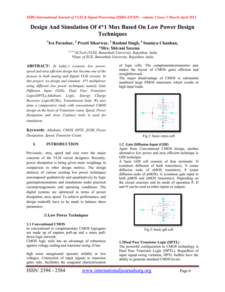
Fig 1: basic cmos cell
1.2 Gate Diffusion Input (GDI)
Apart from Conventional CMOS design, another
alternative low power and area efficient technique is
GDI technique.
A basic GDI cell consists of four terminals- D
(common diffusion of both transistors), N (outer
diffusion node of nMOS transistor), P (outer
diffusion node of pMOS), G (common gate input to
both pMOS and nMOS transistors). Depending on
the circuit structure and its mode of operation P, D
and N can be used as either inputs or outputs.
II.Low Power Techniques
1.1 Conventional CMOS
In conventional or complementary CMOS logicgates
are made up of anpmos pull-up and a nmos pulldown logic network.
CMOS logic style has an advantage of robustness
against voltage scaling and transistor sizing .It has
high noise marginsand operates reliably at low
voltages. Connection of input signals to transistor
gates only, facilitates the usageand characterization
ISSN: 2394 - 2584
Fig 2: basic gdi cell
1.3Dual Pass Transistor Logic (DPTL)
The powerful configuration in CMOS technology is
Dual Pass Transistor Logic (DPTL). Regardless of
input signal-swing variation, DPTL buffers have the
ability to generate standard CMOS levels.
www.internationaljournalssrg.org
Page 6
SSRG International Journal of VLSI & Signal Processing (SSRG-IJVSP) – volume 2 Issue 2 March-April 2015
A basic DPTL structure consists of pMOS and nMOS
transistors connected in parallel.
Dual logic function in DPTL is generated by
exchanging NMOS and PMOS, VDD and GND.
1.5 Energy Charge Recovery Logic(ECRL):
ECRL technology is that in which precharge and
evaluation phase works simultaneously .The circuit
has two NMOS functional blocks and two cross
coupled transistors M1 and M2 of PMOSfor ECRL
adiabatic logic implementation. To recover and reuse
the supplied energy, an AC power supply isused.
Both out and /out are drive a constant load
capacitance independent of the input signal. The full
swing in both precharge and recover phases are
obtained by cross coupled PMOS transistors. The
PMOS transistor gets turned off as the voltage on the
supply clock approaches to │Vtp│
Fig 3: dptl basic cell
1.4 AdiabaticLogic
Adiabatic circuits are low power circuits which
works on the principle of "reversible logic" to
conserve energy.
Unlike CMOS, Adiabatic circuits reduce power
dissipation during switching by following key rules:
In adiabatic logic, the stored energy is given back to
power supply i.e. reversible logic thus reduces the
power. Power clock plays an important role in
principle of operation of adiabatic circuits. The two
major design rules for the adiabatic circuit design
achieved by each phase of power clock :
1. Never turn on a transistor when there is a
voltage potential between the source and
drain.
2. Never turn off a transistor when current is
flowing through it.
Fig 5: ecrl basic cell [7]
III. DESIGNING OF 4*1 MUX USING
DIFFERENT TECHNIQUES
Fig6: multiplexer
Fig5: adiabatic logic [1]
ISSN: 2394 - 2584
www.internationaljournalssrg.org
Page 7
SSRG International Journal of VLSI & Signal Processing (SSRG-IJVSP) – volume 2 Issue 2 March-April 2015
TABLE 1: Truth Table Of 4*1 Mux
SELECTI
ON
LINES
S2 S1
0
0
0
1
1
0
1
1
INPUTS
A
1
0
0
0
B
0
1
0
0
O/P
C
0
0
1
0
D
0
0
0
1
Y
A
B
C
D
3.1 Conventional CMOS
Fig 9: 4*1 mux using gdi
From fig 9 we conclude that GDI technique uses less
number of transistors resulting in less power
dissipation as compared to cmos .
Fig 7: 4*1 mux using cmos
From fig7 we can say that the CMOS technique
utilizes more as large number of transistors are used
resulting in large power dissipation.
Fig:10 GDIwaveform
3.3 Dual Pass Transistor Logic (DPTL)
Fig:8cmoswaveform
3.2 Gate Diffusion Input(GDI)
Fig 11: 4*1 mux using dptl
From fig it is seen that from this technique we get
high speed as compared to other techniques
ISSN: 2394 - 2584
www.internationaljournalssrg.org
Page 8
SSRG International Journal of VLSI & Signal Processing (SSRG-IJVSP) – volume 2 Issue 2 March-April 2015
3.4 Adiabatic Logic
Fig 15: ecrlwaveform
Fig 12: 4*1 Mux using adiabatic logic
From this fig we can say that energy is reusable so
power dissipation is less.
IV. DESIGN METRICES
4.1 Power dissipation:
Static dissipation due to
sub threshold conduction through OFF
transistors
tunneling current through gate oxide
leakage through reverse-biased diodes
contention current in rationed circuits
Dynamic dissipation:
due to charging and discharging of load
capacitances
short circuit current while both
PMOS and NMOS networks are
partially ON
Ptotal= Pstatic+Pdynamic
Fig 13: adiabatic logic waveform
3.5 ECRL LOGIC
…………… (1)
Pdynamic=1/2 (CL*VDD 2 *fc)……(2)
Pstatic = Ioff* VDD……………………….(3)
Where,
CL= load capacitance
VDD=Power supply
fc= Clock frequency
Ioff =leakage current drawn by each switch in off state
4.2Speed : Speed of digital circuits can be found by :
delay
Fig 14: 4*1 mux using ecrl logic
From fig we conclude that it exhibits minimum
power dissipation among all the techniques used.
ISSN: 2394 - 2584
td= (CL * VDD) /Ion…………..(4)
Maximum clock frequency:
fc,max= 1/( td * Ld)……….(5)
where,
CL= load capacitance
www.internationaljournalssrg.org
Page 9
SSRG International Journal of VLSI & Signal Processing (SSRG-IJVSP) – volume 2 Issue 2 March-April 2015
VDD=Power supply
As the number of transistor count in digital circuits
increases, area also increases and vice-versa.
Ion= leakage current drawn by each switch in on state
Ld= logic depth (no of stages through which a
switching event must propogate during one clock
cycle)
4.3Transistor Count:
The number of transistors in the device is called the
transistor count. Transistor count is the most common
measure of integrated circuit size.
According to Moore's Law, the number of transistor
count doubles approximately every two years.
Fig 16 :moore’s law
V.COMPARISION 0F VARIOUS DESIGN TECHNIQUES ON THE BASIS OF DESIGN
METRICES
TABLE 2:
Sr.no
Technique used
1
Transistor count
Speed
Power Dissipation
Area
26
LOW
932uW
MORE
2
CMOS
GDI
6
LOW
1.8570pW
LESS
3
DPTL
6
HIGH
98.655pW
LESS
4
Adiabatic logic
28
HIGH
26.1855pW
MORE
5
Energy charge recovery
logic (ECRL)
26
HIGH
20.06uW
MORE
VI. CONCLUSION
In this paper, the digital circuit 4*1 mux was
implemented by different low power techniques
namely CMOS, GDI, adiabatic, ECRL, DPTL and
transmission gate. The results were simulated using
cadence and comparison has been done for different
ISSN: 2394 - 2584
parameters like power dissipation, speed, area and
transistor count .
The results concluded that as compared to other
proposed techniques, CMOS has more power
dissipation and transistor count. These advantages of
proposed techniques over CMOS make them more
efficient and convenient to be used in digital circuits.
www.internationaljournalssrg.org
Page 10
SSRG International Journal of VLSI & Signal Processing (SSRG-IJVSP) – volume 2 Issue 2 March-April 2015
REFERENCES
[1]. Cmos digital integrated circuits by sung-mo Kang Yusuf
Leblebici “low power cmos logic circuits”pp 481-520
[2]. K. Yano, Y. Sasaki, K. Rikino, and K. Seki, “Top-down passtransistor logic design,” IEEE J. Solid-State Circuits, vol. 31, pp.
792–803, June1996.
[3]. A. P. Chandrakasan, S. Sheng, and R. W. Brodersen, “Lowpower CMOS digital design,” IEEE J. Solid- State Circuits, vol.
27, pp.473– 484, Apr. 1992.
[4]. R. Zimmermann and W. Fichtner, \Low-power logic styles:
CMOS versus pass- transistor logic,"IEEE J. Solid-State Circuits,
vol. 32, no. 7, pp. 1079{1090, Jul. 1997.
[5]. B. Dilli Kumar, M. Bharathi, “Design of Energy Efficient
Arithmetic Circuits Using Charge Recovery Adiabatic Logic” in
International Journal of Engineering Trends and Technology,
2013.
[6] “Gate-diffusion input (GDI) – A technique for low power
design of digital circuits: Analysis and characterization,” in Proc.
Int. Symp. Circuits and Systems (ISCAS), May 2002.
[7]. Sarita, JyotiHooda, ShwetaChawla“design and implementation
of low power 4:1 multiplexer using adiabatic logic”(IJITEE) ISSN:
2278-3075, Volume-2, Issue-6, May 2013.
ISSN: 2394 - 2584
www.internationaljournalssrg.org
Page 11

