The MOSFET - W. Marshall Leach, Jr.
advertisement
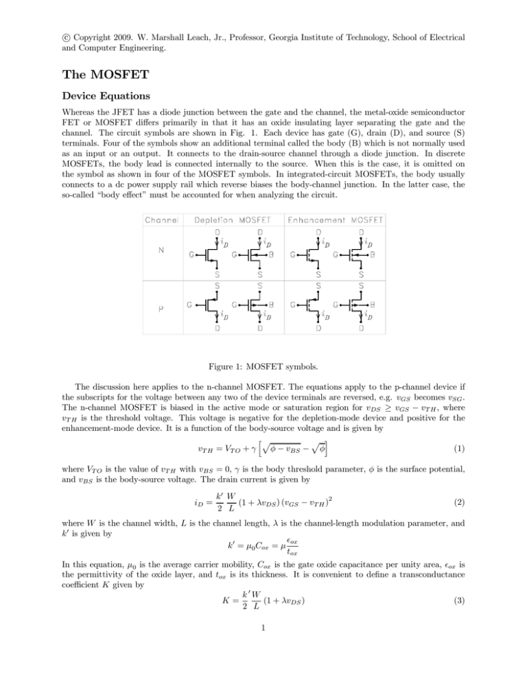
c Copyright 2009. W. Marshall Leach, Jr., Professor, Georgia Institute of Technology, School of Electrical ° and Computer Engineering. The MOSFET Device Equations Whereas the JFET has a diode junction between the gate and the channel, the metal-oxide semiconductor FET or MOSFET differs primarily in that it has an oxide insulating layer separating the gate and the channel. The circuit symbols are shown in Fig. 1. Each device has gate (G), drain (D), and source (S) terminals. Four of the symbols show an additional terminal called the body (B) which is not normally used as an input or an output. It connects to the drain-source channel through a diode junction. In discrete MOSFETs, the body lead is connected internally to the source. When this is the case, it is omitted on the symbol as shown in four of the MOSFET symbols. In integrated-circuit MOSFETs, the body usually connects to a dc power supply rail which reverse biases the body-channel junction. In the latter case, the so-called “body effect” must be accounted for when analyzing the circuit. Figure 1: MOSFET symbols. The discussion here applies to the n-channel MOSFET. The equations apply to the p-channel device if the subscripts for the voltage between any two of the device terminals are reversed, e.g. vGS becomes vSG . The n-channel MOSFET is biased in the active mode or saturation region for vDS ≥ vGS − vT H , where vT H is the threshold voltage. This voltage is negative for the depletion-mode device and positive for the enhancement-mode device. It is a function of the body-source voltage and is given by hp p i vT H = VT O + γ φ − vBS − φ (1) where VT O is the value of vT H with vBS = 0, γ is the body threshold parameter, φ is the surface potential, and vBS is the body-source voltage. The drain current is given by iD = k0 W 2 (1 + λvDS ) (vGS − vT H ) 2 L (2) where W is the channel width, L is the channel length, λ is the channel-length modulation parameter, and k 0 is given by ox k 0 = µ0 Cox = µ tox In this equation, µ0 is the average carrier mobility, Cox is the gate oxide capacitance per unity area, ox is the permittivity of the oxide layer, and tox is its thickness. It is convenient to define a transconductance coefficient K given by k0W K= (3) (1 + λvDS ) 2 L 1 With this definition, the drain current can be written iD = K (vGS − vT H )2 (4) Note that K plays the same role in the MOSFET drain current equation as β plays in the JFET drain current equation. Figure 2 shows the typical variation of drain current with gate-to-source voltage for a constant drainto-source voltage and zero body-to-source voltage. In this case, the threshold voltage is a constant, i.e. vT H = VT O . For vGS ≤ VT O , the drain current is zero. For vGS > VT O , the drain current increases approximately as the square of the gate-to-source voltage. The slope of the curve represents the small-signal transconductance gm , which is defined in the next section. Fig. 3 shows the typical variation of drain current with drain-to-source voltage for a several values of gate-to-source voltage vGS and zero body-tosource voltage vBS . The dashed line divides the triode region from the saturation or active region. In the saturation region, the slope of the curves represents the reciprocal of the small-signal drain-source resistance r0 , which is defined in the next section. Figure 2: Drain current iD versus gate-to-source voltage vGS for constant drain-to-source voltage vDS . Figure 3: Drain current iD versus drain-to-source voltage vDS for constant gate-to-source voltage vGS . Bias Equation Figure 4 shows the MOSFET with the external circuits represented by Thévenin dc circuits. If the MOSFET is in the pinch-off region, the following equations for ID hold: ID = K (VGS − VT H )2 2 (5) VGS = VGG − (VSS + ID RSS ) (6) K = K0 (1 + λVDS ) (7) VDS = (VDD − ID RDD ) − (VSS + ID RSS ) (8) Because this is a set of nonlinear equations, a closed form solution for ID cannot be easily written unless it is assumed that K is not a function of VDS and VT H is not a function of VBS . The former assumption requires the condition λVDS ¿ 1. With these assumptions, the equations can be solved for ID to obtain ID = i2 hp 1 1 + 4KR (V − V − V ) − 1 SS GG SS TH 2 4KRSS (9) Figure 4: MOSFET dc bias circuit. Unless λVDS ¿ 1 and the dependence of VT H on VBS is neglected, Eq. (9) is only an approximate solution. A numerical procedure for obtaining a more accurate solution is to first calculate ID with K = K0 and VT H = VT O . Then calculate VDS and the new values of K and VT H from which a new value for ID can be calculated. The procedure can be repeated until the solution for ID converges. Alternately, computer tools can be used to obtain a numerical solution to the set of nonlinear equations. Small-Signal Models There are two small-signal circuit models which are commonly used to analyze MOSFET circuits. These are the hybrid-π model and the T model. The two models are equivalent and give identical results. They are described below. Hybrid-π Model Let the drain current and each voltage be written as the sum of a dc component and a small-signal ac component as follows: iD = ID + id (10) vGS = VGS + vgs (11) vBS = VBS + vbs (12) vDS = VDS + vds (13) If the ac components are sufficiently small, we can write id = ∂ID ∂ID ∂ID vgs + vbs + vds ∂VGS ∂VBS ∂VDS (14) where the derivatives are evaluated at the dc bias values. Let us define gm = p ∂ID = K (VGS − VT H ) = 2 KID ∂VGS 3 (15) √ ∂ID γ KID √ gmb = = = χgm ∂VBS φ − VBS γ χ= √ 2 φ − VBS · ¸−1 · 0 ¸−1 ∂ID k W VDS + 1/λ 2 = = r0 = λ (VGS − VT H ) ∂VDS 2 L ID (16) (17) (18) The small-signal drain current can thus be written id = idg + idb + vds r0 (19) where idg = gm vgs (20) idb = gmb vbs (21) The small-signal circuit which models these equations is given in Fig. 5. This is called the hybrid-π model. Figure 5: Hybrid-π model of the MOSFET. T Model The T model of the MOSFET is shown in Fig. 6. The resistor r0 is given by Eq. (18). The resistors rs and rsb are given by 1 (22) rs = gm rsb = 1 1 rs = = gmb χgm χ (23) where gm and gmb are the transconductances defined in Eqs. (15) and (16). The currents are given by id = isg + isb + vds r0 vgs = gm vgs rs vbs = = gmb vbs rsb (24) isg = (25) isb (26) The currents are the same as for the hybrid-π model. Therefore, the two models are equivalent. Note that the gate and body currents are zero because the two controlled sources supply the currents that flow through rs and rsb . 4 Figure 6: T model of the MOSFET. Small-Signal Equivalent Circuits Several equivalent circuits are derived below which facilitate writing small-signal low-frequency equations for the MOSFET. We assume that the circuits external to the device can be represented by Thévenin equivalent circuits. The Norton equivalent circuit seen looking into the drain and the Thévenin equivalent circuit seen looking into the source are derived. Several examples are given which illustrate use of the equivalent circuits. Simplified T Model Figure 7 shows the MOSFET T model with a Thévenin source in series with the gate and the body connected to signal ground. We wish to solve for the equivalent circuit in which the sources isg and isb are replaced by a single source which connects from the drain node to ground having the value i0d = i0s . We call this the simplified T model. The first step is to look up into the branch labeled i0s and form a Thévenin equivalent circuit. With i0s = 0, we can use voltage division to write vs(oc) = vtg vtg rsb rs /χ = vtg = rs + rsb rs + rs /χ 1+χ (27) With vtg = 0, the resistance rs0 seen looking up into the branch labeled i0s is rs0 = rs krsb = rs 1 = 1+χ (1 + χ) gm (28) Figure 7: T model with Thévenin source connected to the gate and the body connected to signal ground. The simplified T model is shown in Fig.8. Compared to the corresponding circuit for the BJT, the MOSFET circuit replaces vtb with vtg / (1 + χ) and re0 with rs0 = rs / (1 + χ). Because the gate current is zero, set α = 1 and β = ∞ in converting any BJT formulas to corresponding MOSFET formulas. The simplified T model is derived with the assumption that the body lead connects to signal ground. In the case 5 that the body lead connects to the source lead, it follows from Fig. 7 that isb = 0. Connecting the body to the source is equivalent to setting χ = 0 in the MOSFET equations. Figure 8: Simplified T model. Norton Drain Circuit Figure 9(a) shows the MOSFET with Thévenin sources connected to its gate and source leads and the body lead connected to signal ground. The Norton equivalent circuit seen looking into the drain can be obtained from the Norton equivalent circuit seen looking into the BJT collector by replacing Gmb with Gmg , Gme with Gms , and ric with rid . The factor 1/ (1 + χ) must be incorporated into the equation for Gmg . To convert the formulas, replace Rtb with Rtg , Rte with Rte , Rtc with Rtd , re0 with rs0 , set α = 1, and set β = ∞. The circuit is given in Fig. 9(b), where id(sc) and rid are given by id(sc) = Gmg vtg − Gms vts µ ¶ Rts rid = r0 1 + 0 + Rts rs (29) (30) The transconductances Gmg and Gms are given by Gmg = 1 r0 1 0 1 + χ rs + Rts kr0 r0 + Rts (31) 1 Rts + rs0 kr0 (32) 1 1 = gm 1 + χ rs0 (33) 1 1 = (1 + χ) gm + rs0 kr0 r0 (34) 1 1 0 1 + χ rs + Rts (35) Gms = The equations for the case where the body is connected to the source are obtained by setting χ = 0. For the case Rts = 0, the equations for Gmg and Gms reduce to Gmg = Gms = For the case r0 À Rts and r0 À rs0 , we can write Gmg = and Gms = rs0 1 + Rts (36) The value of id(sc) calculated with these approximations is simply the value of i0s calculated with r0 considered to be an open circuit. The term “r0 approximations” is used in the following when r0 is neglected in calculating id(sc) but not neglected in calculating rid . 6 Figure 9: (a) MOSFET with Thévenin sources connected to the gate and source. (b) Norton drain circuit. Thévenin Source Circuit Figure 10(a) shows the MOSFET with a Thévenin source connected to its gate, the body lead connected to signal ground, and the external drain load represented by the resistor Rtd . The Thévenin equivalent circuit seen looking into the source can be obtained from the Thévenin equivalent circuit seen looking into the BJT emitter by replacing ve(oc) with vs(oc) , rie with ris , vtb with vtg / (1 + χ), Rtb with Rtg , Rtc with Rtd , re0 with rs0 , setting α = 1, and setting β = ∞. The circuit is given in Fig. 10(b), where vs(oc) and ris are given by vs(oc) = vtg r0 1 + χ r0 + rs0 (37) r0 + Rtd r0 + rs0 (38) ris = rs0 The equations for the case where the body is connected to the source are obtained by setting χ = 0. Figure 10: (a) MOSFET with Thévenin source connected to gate. (b) Thévenin source circuit. The r0 Approximations The r0 approximations approximate r0 as an open circuit in all equations except the one for rid . In this case, the equations for id(sc) , Gmg , Gms , rid , vs(oc) , and ris are 1 1 1 Gms = 0 0 1 + χ rs + Rts rs + Rts µ ¶ Rts r0 + rs0 kRts or + Rts = = r0 1 + 0 1 − Rts / (rs0 + Rts ) rs vtg ve(oc) = ris = rs0 1+χ id(sc) = i0d = Gmg vtg − Gms vts rid Gmg = 7 (39) (40) (41) The simplified T model, the hybrid π model, and the T model, respectively, are given Figs. 11 - 13. If r0 = ∞, then rid is an open circuit in each. Because r0 no longer connects to the source, there is only one source current and is = i0s . Figure 11: Simplified T model with r0 approximations. Figure 12: Hybrid π model with the r0 approximations. Figure 13: T model with the r0 approximations. Summary of Models Figure 14 summarizes the four equivalent circuits derived above. For the case where the body is connected to the source, set χ = 0 in the equations. Example Amplifier Circuits This section describes several examples which illustrate the use of the small-signal equivalent circuits derived above to write by inspection the voltage gain, the input resistance, and the output resistance of several amplifier circuits. 8 Figure 14: Summary of the small-signal equivalent circuits. Set χ = 0 if the body is connected to the source. Common-Source Amplifier Figure 15(a) shows a common-source amplifier. The active device is M1 . Its load consists of a current-mirror active load consisting of M2 and M3 . The current source IQ sets the drain current in M3 which is mirrored into the drain of M2 . Because the source-to-drain voltage of M2 is larger than that of M3 , the Early effect causes the dc drain current in M2 to be slightly larger than IQ . The input voltage can be written vI = VB +vi , where VB is a dc bias voltage which sets the drain current in M1 . It must be equal to the drain current in M2 in order for the dc component of the output voltage to be stable. In any application of the circuit, VB would be set by feedback. Looking out of the drain of M1 , the resistance to ac signal ground is Rtd1 = r02 . Figure 15: (a) CMOS common-source amplifier. (b) Common-drain amplifier. The voltage gain of the circuit can be written id1(sc) vo vo = = Gmg1 × (−rid1 kr02 ) vi vi id1(sc) (42) where Gmg1 is given by Eq. (31), rid1 is given by Eq. (30), and Rts1 = RS . The body effect cancels if RS = 0. The output resistance is given by rout = rid1 kr02 9 (43) Common-Drain Amplifier Figure 15(b) shows a common-drain amplifier. The active device is M1 . Its load consists of a current-mirror active load consisting of M2 and M3 . The current source IQ sets the drain current in M3 which is mirrored into the drain of M2 . As with the common-source amplifier, the Early effect makes the drain current in M2 slightly larger than that in M3 . The input voltage can be written vI = VB + vi , where VB is a dc bias voltage which sets the dc component of the output voltage. Looking out of the source of M1 , the resistance to ac signal ground is Rts1 = r02 . The voltage gain can be written vs1(oc) vo vo 1 r01 r02 = = 0 r vi vi vs1(oc) 1 + χ1 r01 + rs1 02 + ris1 (44) where ris1 is given by Eq. (38). The output resistance is given by rout = ris1 kr02 (45) Common-Gate Amplifier Figure 16(a) shows a common-gate amplifier. The active device is M1 . Its load consists of a current-mirror active load consisting of M2 and M3 . The current source IQ sets the drain current in M3 which is mirrored into the drain of M2 . As with the common-source amplifier, the Early effect makes the drain current in M2 slightly larger than that in M3 . The dc voltage VB is a dc bias voltage which sets the drain current in M1 which must be equal to the drain current in M2 in order for the dc component of the output voltage to be stable. In any application of the circuit, VB would be set by feedback. Looking out of the drain of M1 , the resistance to ac signal ground is Rtd1 = r02 . Figure 16: (a) CMOS Common-gate amplifier. (b) CMOS differential amplifier. The voltage gain of the circuit can be written id1(sc) v0 vo = = −Gms1 × (−rid1 kr02 ) vi vi id1(sc) (46) where Gms1 is given by Eq. (32) and rid1 is given by Eq. (30). The input and output resistances are given by rin = Ri + ris1 (47) rout = rid1 kr02 where ris1 is given by Eq. (38). 10 (48) Differential Amplifier A MOS differential amplifier with an active current-mirror load is shown in Fig. 16(b). The object is to determine the Norton equivalent circuit seen looking into the output To do this, the output is connected to ac signal ground, which is indicated by the dashed line. It will be assumed that the Early effect can be neglected in all devices in calculating io(sc) but not neglected in calculating rout , i.e. we use the r0 approximations. We can write io(sc) = id1(sc) − id3(sc) = id1(sc) − id4(sc) = id1(sc) − id2(sc) (49) Because the tail supply is a current source, the currents id1 and id2 can be calculated by replacing vi1 and vi2 with their differential components. In this case, the ac signal voltage at the sources of M1 and M2 is zero. Let vi1 = vi(d) /2 and vi2 = −vi(d) /2, where vid = vi1 − vi2 . It follows by symmetry that id2(sc) = −id1(sc) so that io(sc) is given by io(sc) = 2id1(sc) = 2Gmg1 = 2 vi(d) 2 1 1 vi(d) = gm1 (vi1 − vi2 ) (1 + χ) rs0 2 (50) where Eq. (35) with Rts = 0 is used for Gmg . Note that the body effect cancels. This is because the source-to-body ac signal voltage is zero for the differential input signals. The output resistance is given by rout = r01 kr03 (51) Note that rid1 = r01 because Rts1 = Rts2 = 0 for the differential input signals. Small-Signal High-Frequency Models Figures 17 and 18 show the hybrid-π and T models for the MOSFET with the gate-source capacitance cgs , the source-body capacitance csb , the drain-body capacitance cdb , the drain-gate capacitance cdg , and the gate-body capacitance cgb added. These capacitors model charge storage in the device which affect its high-frequency performance. The first three capacitors are given by cgs = csb = cdb = 2 W LCox 3 csb0 (1 + VSB /ψ 0 ) cdb0 (52) 1/2 (1 + VDB /ψ 0 )1/2 (53) (54) where VSB and VDB are dc bias voltages; csb0 and cdb0 are zero-bias values; and ψ 0 is the built-in potential. Capacitors cgd and cgb model parasitic capacitances. For IC devices, cgd is typically in the range of 1 to 10 fF for small devices and cgb is in the range of 0.04 to 0.15 fF per square micron of interconnect. Figure 17: High-frequency hybrid-π model. 11 Figure 18: High-frequency T model. 12
