UNIVERSITY OF CALIFORNIA College of Engineering
advertisement
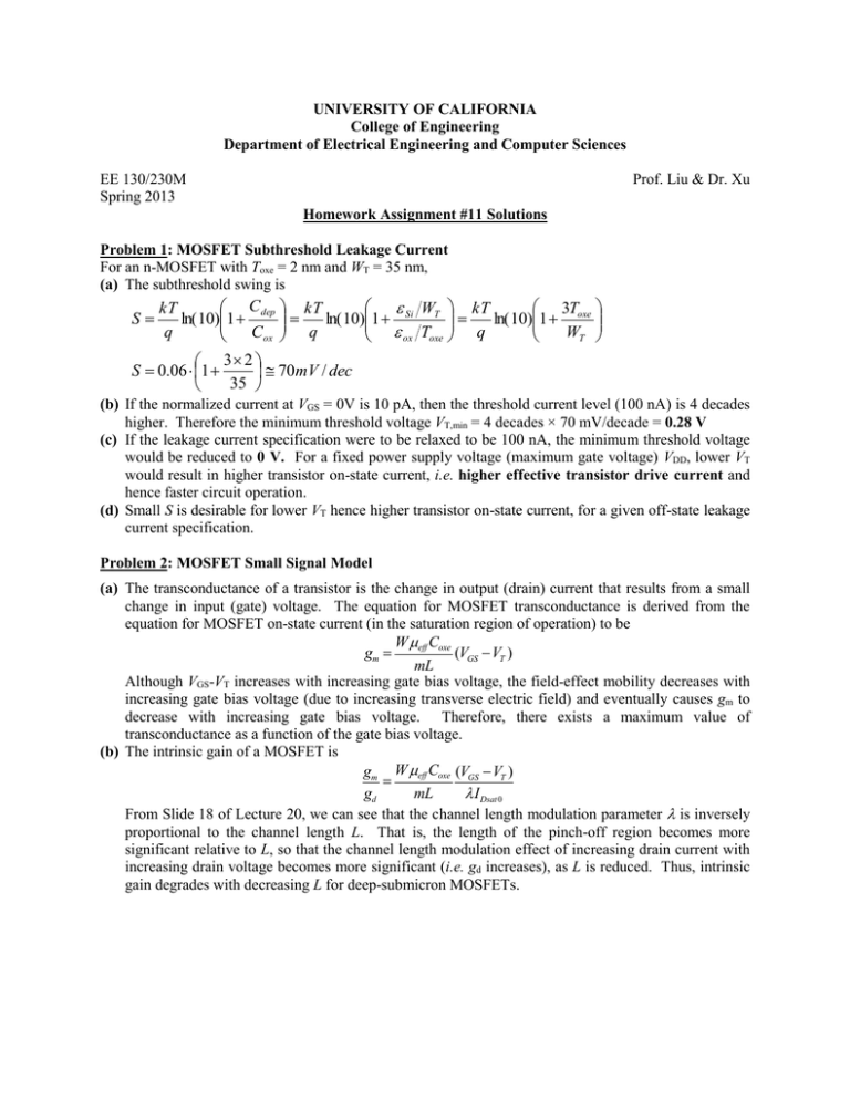
UNIVERSITY OF CALIFORNIA College of Engineering Department of Electrical Engineering and Computer Sciences EE 130/230M Spring 2013 Prof. Liu & Dr. Xu Homework Assignment #11 Solutions Problem 1: MOSFET Subthreshold Leakage Current For an n-MOSFET with Toxe = 2 nm and WT = 35 nm, (a) The subthreshold swing is Cdep kT W kT 3T kT ln( 10)1 ln( 10)1 Si T ln( 10)1 oxe q Cox q WT ox Toxe q 3 2 S 0.06 1 70mV / dec 35 S (b) If the normalized current at VGS = 0V is 10 pA, then the threshold current level (100 nA) is 4 decades higher. Therefore the minimum threshold voltage VT,min = 4 decades × 70 mV/decade = 0.28 V (c) If the leakage current specification were to be relaxed to be 100 nA, the minimum threshold voltage would be reduced to 0 V. For a fixed power supply voltage (maximum gate voltage) VDD, lower VT would result in higher transistor on-state current, i.e. higher effective transistor drive current and hence faster circuit operation. (d) Small S is desirable for lower VT hence higher transistor on-state current, for a given off-state leakage current specification. Problem 2: MOSFET Small Signal Model (a) The transconductance of a transistor is the change in output (drain) current that results from a small change in input (gate) voltage. The equation for MOSFET transconductance is derived from the equation for MOSFET on-state current (in the saturation region of operation) to be W meff Coxe gm = (VGS -VT ) mL Although VGS-VT increases with increasing gate bias voltage, the field-effect mobility decreases with increasing gate bias voltage (due to increasing transverse electric field) and eventually causes gm to decrease with increasing gate bias voltage. Therefore, there exists a maximum value of transconductance as a function of the gate bias voltage. (b) The intrinsic gain of a MOSFET is gm W meff Coxe (VGS -VT ) = gd mL l I Dsat 0 From Slide 18 of Lecture 20, we can see that the channel length modulation parameter is inversely proportional to the channel length L. That is, the length of the pinch-off region becomes more significant relative to L, so that the channel length modulation effect of increasing drain current with increasing drain voltage becomes more significant (i.e. gd increases), as L is reduced. Thus, intrinsic gain degrades with decreasing L for deep-submicron MOSFETs. Problem 3: Velocity Saturation (a) First, we need to find the effective electron mobility, eff . In order to do so, we need to find the effective transverse electric field in the inversion layer: VGS +VT + 0.2V 1.0V + 0.3V + 0.2V 1.5V = = = 0.83MV / cm 6Toxe 6 ´ 3nm 18 ´10-7 cm From the plot on Slide 4 of Lecture 20, meff » 260cm2 / V × s The which electric Esat 2 vsat eff field strength at the electron velocity reaches saturation is 2(8 10 cm / s ) 6.15 104V / cm 6.15 104V / cm 2 260cm / V s 6 The bulk charge parameter, m =1+ 3Toxe 3´ 3 =1+ =1.18 WT 50 (i) For L = 1 m: -1 VDsat -1 æ m æ 1.18 ö 1 ö 1 -1 =ç + + = (1.69 + 0.16) = 0.54V ÷ =ç 5 -4 ÷ è 1- 0.3 0.615 ´10 ´10 ø è VGS -VT Esat L ø æ V -V ö ( Esat L = 6.15) >> çè GS T = 0.59 ÷ø m \This MOSFET is a long-channel device. (ii) For L = 0.1m: -1 VDsat æ 1.18 ö 1 -1 =ç + = (1.68 +1.63) = 0.3V 5 -5 ÷ è 0.7 0.615´10 ´10 ø æ VGS -VT ö = 0.59 ÷ ø m ( Esat L = 0.615) @ çè This MOSFET is a short-channel device. (b) VDsat m 1 V V E L T sat GS 1 VDsat will decrease with decreasing (VGS-VT)/m or decreasing EsatL. (i) (ii) When Toxe decreases, VT decreases (because Cox increases so that the voltage dropped across the gate oxide, Qdep/Cox, decreases) and thus (VGS- VT) increases. Consequently, VDsat increases. When (VGSVT) gets smaller, VDsat decreases because it becomes easier to pinch off the inversion-layer channel at the drain end. Problem 4: MOSFET Short-Channel Effect (a) For a n-channel MOSFET with channel dopant concentration NA = 41017/cm3, effective oxide thickness Toxe = 3 nm, source/drain junction depth rj = 0.05 m: The threshold voltage shift, DVT = -qN AWT rj 2W ( 1+ T -1) Coxe L rj Here, F F = (kT / q)ln(N A / ni ) = 0.026 * ln(4 ´10 7 ) = 0.455V WT = 2e si | 2F F | 2 ´10-12 ´ | 2 ´ 0.455 | = = 53nm qN A 1.6 ´10 -19 ´ 4 ´1017 Now, i) at L=1m m, DVT = -qN AWT rj 2W -1.6 ´10 -19 ´ 4 ´1017 ´ 53´10 -7 ´ 5 ´10-6 1 2 ´ 53 ( 1+ T -1) = ( 1+ -1) -7 -4 eox 3´10 L rj 10 50 -14 Toxe 3.45´ 8.854 ´10 -1.696 ´10-12 1 (0.766) = -1.274 ´10-2 V = -12.74mV 1.02 ´10-6 10-4 ii) at L=0.05 m m, DVT = DVT = -1.696 ´10-12 1 (0.766) = -0.2548V = -254.8mV -6 1.02 ´10 0.05 ´10-4 From these calculations of VT it can be seen that the short channel effect (“VT roll-off”) becomes more severe at shorter gate lengths. (b) For a higher value of drain voltage, the drain junction depletion width is larger; so the drain effectively supports a larger fraction of the depletion region charge underneath the gate electrode. Thus, the short channel effect is enhanced and therefore |VT| decreases more rapidly with decreasing L.

