Buck Converter 3-1-1 Circuit diagram and key waveforms
advertisement
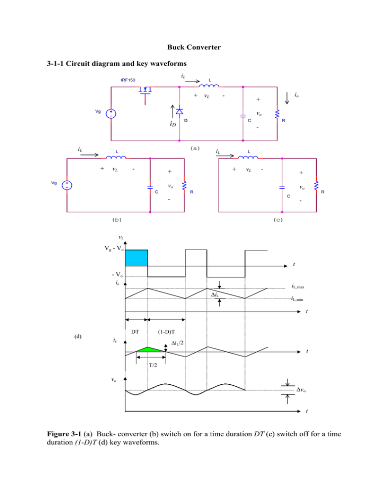
Buck Converter 3-1-1 Circuit diagram and key waveforms iL IRF150 L + vL - Vg vo iD iL D C vL - iL L + + Vg R - (a) L + io + vL - + vo C vo R C (b) R - (c) vL Vg - Vo t - Vo iL iL,max ∆iL iL,min t (d) DT (1-D)T ic ∆iL/2 t T/2 vo ∆vo t Figure 3-1 (a) Buck- converter (b) switch on for a time duration DT (c) switch off for a time duration (1-D)T (d) key waveforms. 3-1-2 Circuit description and operation Circuit description. The three basic dc-dc converters use a pair of switches, usually one controlled (eg. MOSFET) and one uncontrolled (ie. diode), to achieve unidirectional power flow from input to output. The converters also use one capacitor and one inductor to store and transfer energy from input to output. They also filter or smooth voltage and current. The dc-dc coverters can have two distinct modes of operation: Continuous conduction mode (CCM) and discontinuous conduction mode (DCM). In practice, a converter may operate in both modes, which have significantly different characteristics. Therefore, a converter and its control should be designed based on both modes of operation. However, for this course we only consider the dc-dc converters operated in CCM. Circuit Operation. When the switch is on for a time duration DT, the switch conducts the inductor current and the diode becomes reverse biased. This results in a positive voltage vL = Vg – Vo across the inductor. This voltage causes a linear increase in the inductor current iL. When the switch is turned off, because of the inductive energy storage, iL continues to flow. This current now flows through the diode, and vL = -Vo for a time duration (1-D)T until the switch is turned on again. 3-1-3 Analytical expressions for Vo , ∆iL, and ∆vo Vg Assumptions made about the operation of the converter are as follows: • The circuit is operating in the steady state • The circuit is operating in the CCM • The capacitor is large enough to assume a constant output voltage • The component are ideal. Equating the integral of the inductor voltage over one time period to zero yields ∫ T 0 v L dt = ∫ t on 0 t off v L dt + ∫ v L dt = 0 0 (V g − V ) o × DT + ( −Vo ) × (1 − D )T = 0 Vo = DV g or Vo =D Vg Assuming a lossless circuit, Pg = Po, Therefore V g I g = Vo I o And I o Vg 1 = = I g Vo D For a buck converter, it is obvious that I L = Io 1 DT v L dt L ∫0 1 = [ Shaded area under waveform v L (Area A)] L 1 = (V g − Vo ) × DT L ∆i L = From ∆iL we can obtain iL,min and iL, max ∆i L 2 ∆i L = IL + 2 i L ,min = I L − i L ,max To obtain the average inductor current, we can use the relationship I L = Io = Vo R The peak-peak output voltage ripple, ∆vo. From the information of the capacitor current, ic, we can obtain ∆vo. ∆vo = ∆vc = 1 ic dt C∫ 1 [Shaded area under waveform ic ] L 1 1 T ∆i = × × × L C 2 2 2 = therefore ∆vo = ∆i L 8 fC 3-1-4 CCM/DCM boundary condition Being at the boundary between the continuous and the discontinuous mode, by definition, the inductor current iL goes to zero at the end of the off period. At this boundary, the average inductor current is ∆i IL = L 2 the minimum inductor current, iL, min = 0 and the maximum inductor curren iL, max = ∆iL. Vg - Vo vL iL DT (1-D)T t -Vo Vo 1 1 and ∆i L = (V g − Vo ) DT = Vo (1 − D)T . R L L ∆i L Equation at the CCM/DCM boundary, I L = , can be used to determine the combination 2 of L, f and R that will result in CCM. The minimum load current required for CCM operation is: ∆i IL = Io = L 2 1 ∴I o ,min = Vo (1 − D)T 2L We know that for buck converters I L = I o = If the desired switching frequency f and load resistance R are established, the minimum inductor current required for CCM is: ∆i IL = L 2 Vo 1 Vo (1 − D)T = R 2L (1 − D)T × R ∴ Lmin = 2 (1 − D) R = 2f If the desired value of the inductor L and the load resistance R are established, the minimum switching frequency required for CCM is f min = (1 − D) R 2L If the desired switching frequency and the value of the inductor L are established, the minimum load resistance required for CCM is 2 fL Rmin = (1 − D) -tammat-

