Darlington`s Contributions to Transistor Circuit Design
advertisement

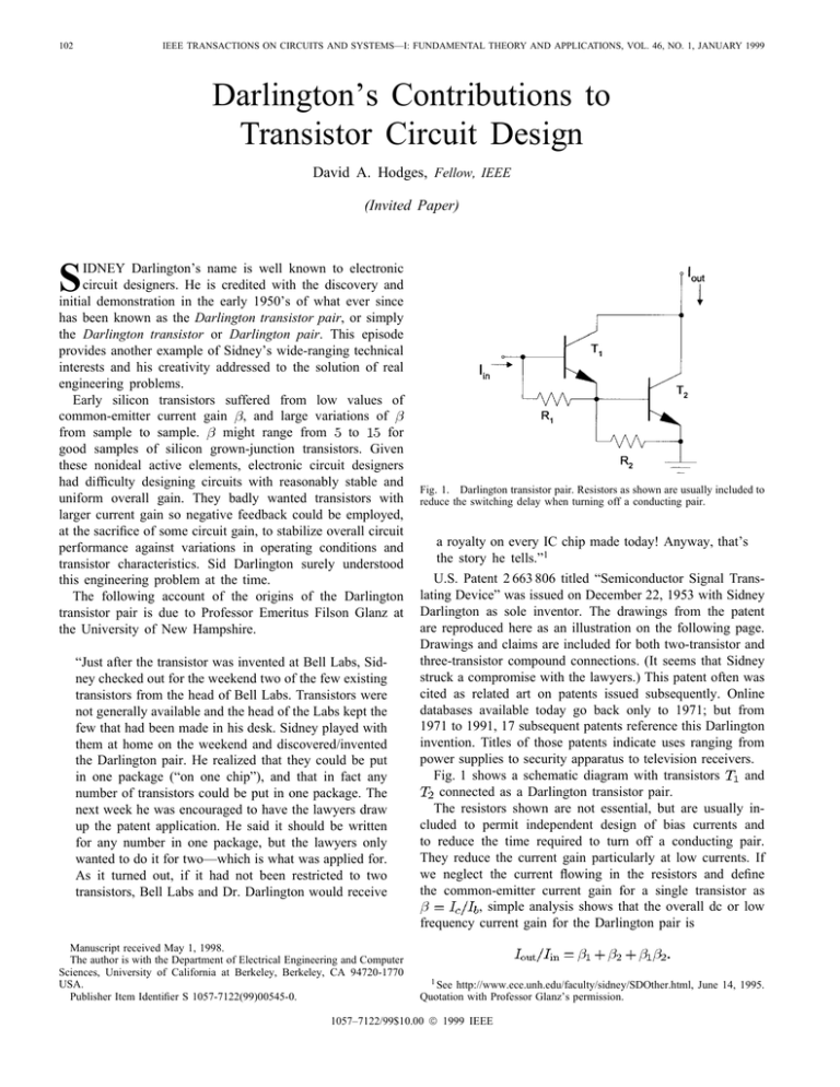
102 IEEE TRANSACTIONS ON CIRCUITS AND SYSTEMS—I: FUNDAMENTAL THEORY AND APPLICATIONS, VOL. 46, NO. 1, JANUARY 1999 Darlington’s Contributions to Transistor Circuit Design David A. Hodges, Fellow, IEEE (Invited Paper) S IDNEY Darlington’s name is well known to electronic circuit designers. He is credited with the discovery and initial demonstration in the early 1950’s of what ever since has been known as the Darlington transistor pair, or simply the Darlington transistor or Darlington pair. This episode provides another example of Sidney’s wide-ranging technical interests and his creativity addressed to the solution of real engineering problems. Early silicon transistors suffered from low values of common-emitter current gain , and large variations of from sample to sample. might range from to for good samples of silicon grown-junction transistors. Given these nonideal active elements, electronic circuit designers had difficulty designing circuits with reasonably stable and uniform overall gain. They badly wanted transistors with larger current gain so negative feedback could be employed, at the sacrifice of some circuit gain, to stabilize overall circuit performance against variations in operating conditions and transistor characteristics. Sid Darlington surely understood this engineering problem at the time. The following account of the origins of the Darlington transistor pair is due to Professor Emeritus Filson Glanz at the University of New Hampshire. “Just after the transistor was invented at Bell Labs, Sidney checked out for the weekend two of the few existing transistors from the head of Bell Labs. Transistors were not generally available and the head of the Labs kept the few that had been made in his desk. Sidney played with them at home on the weekend and discovered/invented the Darlington pair. He realized that they could be put in one package (“on one chip”), and that in fact any number of transistors could be put in one package. The next week he was encouraged to have the lawyers draw up the patent application. He said it should be written for any number in one package, but the lawyers only wanted to do it for two—which is what was applied for. As it turned out, if it had not been restricted to two transistors, Bell Labs and Dr. Darlington would receive Manuscript received May 1, 1998. The author is with the Department of Electrical Engineering and Computer Sciences, University of California at Berkeley, Berkeley, CA 94720-1770 USA. Publisher Item Identifier S 1057-7122(99)00545-0. Fig. 1. Darlington transistor pair. Resistors as shown are usually included to reduce the switching delay when turning off a conducting pair. a royalty on every IC chip made today! Anyway, that’s the story he tells.”1 U.S. Patent 2 663 806 titled “Semiconductor Signal Translating Device” was issued on December 22, 1953 with Sidney Darlington as sole inventor. The drawings from the patent are reproduced here as an illustration on the following page. Drawings and claims are included for both two-transistor and three-transistor compound connections. (It seems that Sidney struck a compromise with the lawyers.) This patent often was cited as related art on patents issued subsequently. Online databases available today go back only to 1971; but from 1971 to 1991, 17 subsequent patents reference this Darlington invention. Titles of those patents indicate uses ranging from power supplies to security apparatus to television receivers. and Fig. 1 shows a schematic diagram with transistors connected as a Darlington transistor pair. The resistors shown are not essential, but are usually included to permit independent design of bias currents and to reduce the time required to turn off a conducting pair. They reduce the current gain particularly at low currents. If we neglect the current flowing in the resistors and define the common-emitter current gain for a single transistor as , simple analysis shows that the overall dc or low frequency current gain for the Darlington pair is 1 See http://www.ece.unh.edu/faculty/sidney/SDOther.html, June 14, 1995. Quotation with Professor Glanz’s permission. 1057–7122/99$10.00 1999 IEEE HODGES: DARLINGTON’S CONTRIBUTIONS TO TRANSISTOR CIRCUIT DESIGN Thus at low frequencies the Darlington pair is approximately equivalent to a single transistor with a current gain greater than . Electronic circuit designers welcomed the improvement in current gain. Unfortunately but not surprisingly, high fre- 103 quency analysis shows that the Darlington pair has much more phase shift than a single transistor. While a single transistor amplifier stage usually is unconditionally stable when negative feedback is applied, this is not true of a single-stage amplifier 104 IEEE TRANSACTIONS ON CIRCUITS AND SYSTEMS—I: FUNDAMENTAL THEORY AND APPLICATIONS, VOL. 46, NO. 1, JANUARY 1999 using a Darlington pair. Conventional two-stage commonemitter transistor amplifiers are more easily rendered stable with negative feedback than single-stage amplifers using a Darlington pair. Therefore, the applications for Darlington pairs have been largely in noncritical circuits not requiring use of feedback. Another limitation is that the minimum voltage drop through the device when conducting must be greater than the base–emitter voltage (about 0.8 V) of the second transistor. When switching large currents, the power wasted by this voltage drop can become an issue. The corresponding voltage drop for a simple common-emitter transistor switch is about 0.2 V. The fact that the two transistors of a Darlington pair share a common collector region provokes the question of whether Sidney anticipated the development of the integrated circuit. Sidney’s patent in fact diagrams and claims a transistor pair sharing a single n-type semiconductor region forming the common collector for a Darlington pair. A jumper wire is shown making the connection between the emitter of one and the base of the other. At that time, the interconnecting jumper would have been applied by a manually controlled wire-bonding operation, one pair at a time. Modern planar integrated circuits readily provide batch-interconnected bipolar transistors sharing a common collector region. One concludes that Sidney conceived some but not all of the essential features of a modern integrated circuit. An Internet search for "Darlington transistor" shows that even to this day there are dozens of commercial devices so identified, typically featuring a current gain of 1000 or more. They are used primarily for relay drivers and in other applications requiring simplicity and high gain. For example, they are widely used to actuate solenoid-driven flippers and flashing lights in electromechanical pinball machines. A logic signal of a few milliamperes from a microprocessor, amplified by a Darlington transistor, easily switches an ampere or more at 50 V on a time scale measured in milliseconds, as required for actuating a solenoid or a tungsten lamp. Sidney Darlington made at least one other excursion into the world of transistor circuit design. According to Dr. Franklin Blecher, who joined Bell Laboratories around 1952, Sidney once designed, built, and demonstrated a complete three-stage direct-coupled transistor amplifier of a sort that might be suitable for use in a hearing aid. This circuit used single transistors, not Darlington pairs. Properly designed negative feedback, stabilizing the gain and dc operating point, was included.2 While this was an original undertaking for Sid, it turned out that others had demonstrated such circuits earlier. Sidney Darlington was a person of great curiosity and originality, armed with the best modern scientific and engineering knowledge. The scope of his creative accomplishments is an inspiration to all who knew him. David A. Hodges (S’59–M’65–SM’71–F’77) received the B.E.E. degree from Cornell University, Ithaca, NY, and the M.S. and Ph.D. degrees from the University of California at Berkeley. From 1966 to 1970 he worked at Bell Telephone Laboratories. He was Professor of Electrical Engineering and Computer Science at University of California at Berkeley from 1970 to 1998. He is now Professor in the Graduate School and Daniel M. Tellep Distinguished Professor Emeritus. He served as Dean of Berkeley’s College of Engineering from 1990 to 1996. He was active in teaching and research on microelectronics technology and design. Since 1984 his research centered on semiconductor manufacturing systems. He serves as a Director of Mentor Graphics Corporation, Silicon Image, Inc., and the International Computer Science Institute. Prof. Hodges was the founding editor of the IEEE TRANSACTIONS ON SEMICONDUCTOR MANUFACTURING, a past editor of the IEEE JOURNAL OF SOLID-STATE CIRCUITS, and a past Chairman of the International Solid-State Circuits Conference. He was the recipient of the 1997 IEEE Education Medal. He is a member of the National Academy of Engineering. 2 Franklin H. Blecher, private communication, April 1, 1998.


