(I) (Flip-Flops) Implement a JK flip-flop with a T flip
advertisement
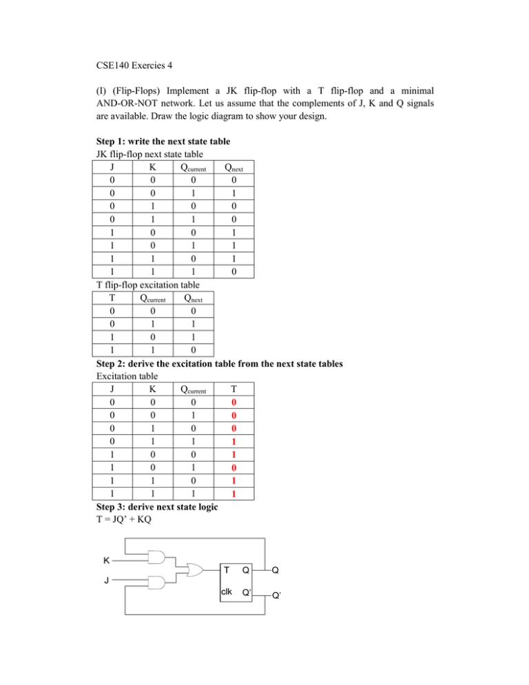
CSE140 Exercies 4 (I) (Flip-Flops) Implement a JK flip-flop with a T flip-flop and a minimal AND-OR-NOT network. Let us assume that the complements of J, K and Q signals are available. Draw the logic diagram to show your design. Step 1: write the next state table JK flip-flop next state table J K Qcurrent Qnext 0 0 0 0 0 0 1 1 0 1 0 0 0 1 1 0 1 0 0 1 1 0 1 1 1 1 0 1 1 1 1 0 T flip-flop excitation table T Qcurrent Qnext 0 0 0 0 1 1 1 0 1 1 1 0 Step 2: derive the excitation table from the next state tables Excitation table J K Qcurrent T 0 0 0 0 0 0 1 0 0 1 0 0 0 1 1 1 1 0 0 1 1 0 1 0 1 1 0 1 1 1 1 1 Step 3: derive next state logic T = JQ’ + KQ (II) (Design Specification) Write the state table of the sequential circuit as the following figure. Q1 Q0 From the circuit we directly get T=x J = Q1Q0’ K = Q1’+Q0’ y = Q1+Q0 We use these equations to get Q1(t+1) and Q0(t+1): Q1 Q0 T Q1(t+1) J K Q0(t+1) 00 0 0 0 0 1 00 1 1 0 0 1 01 0 0 0 0 1 01 1 1 0 0 1 10 0 1 1 1 1 10 1 0 1 1 1 11 0 1 1 0 0 11 1 0 1 0 0 Finally, we get the state table: Next sate Q1 Q0 X=0 X=1 00 00 10 01 00 10 10 11 01 11 11 01 Output (y) X=0 X=1 0 0 1 1 1 1 1 1 (III) A state machine is described by the following state equations. (1). Write the state table. Q1 Q0 00 01 10 11 Next sate X=0 X=1 01 10 01 00 01 11 01 01 Output (y) X=0 X=1 0 0 0 0 0 0 1 1 (2). Design the system with two JK flip-flops and a minimal AND-OR-NOT network. Derive the excitation table: Current Next X J1 K1 J0 K0 state state (Q1 Q0) (Q1 Q0) 0 00 01 0 1 0 01 01 0 0 0 10 01 1 1 0 11 01 1 0 1 00 10 1 0 1 01 00 0 1 1 10 11 0 1 1 11 01 1 0 Derive the next state logic: J1 = Q0’ X K1=X’ + Q0 J0 = Q1 + X’ K0= Q1’ X X J SET Q FF1 K J CLR SET Q Q FF0 K CLR Q Y (IV) In the following circuit, each flip flop has a setup time of 75ps, a hold time of 30ps, a clock-to-Q maximum delay of 80ps, and a clock-to-Q minimum delay of 55ps. Each AND gate has a propagation delay of 70ps and a contamination delay of 55ps, while the NOR gate has a propagation delay of 85ps and a contamination delay of 65ps. CLK CLK a) If there is no clock skew, what is the maximum operating frequency of this circuit? ≥ The constraint is: Tc Tpcq + Tpd + Tsetup In this circuit, the longest path contains the NOR and two AND gates. Therefore, we have: Tc 80+ 85 + 2*70 + 75 = 380 ps Max Frequency = 1/380ps = 2.63 GHz. ≥ b) How much clock skew can the circuit tolerate before it might experience a hold time violation? ≥ The constraint is: Tccq + Tcd Thold + Tskew In this circuit, the shortest path contains only the AND gate at the bottom. Therefore we have: 55 + 55 30 + Tskew Tskew 80 ps ≥ ≤ c) Redesign the circuit so that it can be operated at 3GHz frequency. How much clock skew can your circuit tolerate before it might experience a hold time violation? We can put the second and before the first end since ((a+b)’c)d = (a+b)’(cd) CLK CLK Now the longest path contains one NOR and one AND gate. Tc 80+ 85 + 70 + 75 = 310 ps Max Frequency = 1/310ps = 3.22 GHz. The shortest paths contains only the NOR gate. 55 + 65 30 + Tskew Tskew 0 ps ≥ ≥ ≤ (V) Given a three-input Boolean function f(a; b; c) = Pm(0; 2; 4; 6; 7) + Pd(1). a. Implement the function using a minimal network of 2:4 decoders and OR gates. F = c’+ab c' 1 F 0 1 2 3 I S1S0 a b b. Implement the function using a minimal network of 4:1 multiplexers. F = c’(a’b’+a’b+ab’)+ab = c’(a’b+ab’)+ab 1 c' c' 1 0 1 2 3 // utilize the don’t care a’b’c O F S1S0 ab c. Implement the function using a minimal network of 2:1 multiplexers.
