TB389: PCB Land Pattern and Surface Mount Guidelines for
advertisement

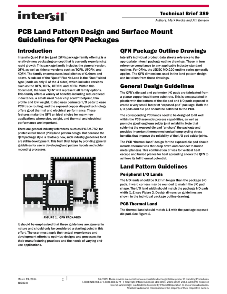
Technical Brief 389 Authors: Mark Kwoka and Jim Benson PCB Land Pattern Design and Surface Mount Guidelines for QFN Packages Introduction QFN Package Outline Drawings Intersil's Quad Flat No Lead (QFN) package family offering is a relatively new packaging concept that is currently experiencing rapid growth. This package family includes the general version, QFN, as well as thinner versions such as TQFN, UTQFN, and XQFN. The family encompasses lead pitches of 0.4mm and above. A sub-set of the "Quad" Flat No Lead is the "Dual" sided type (leads on only 2 of the 4 sides) which includes versions such as the DFN, TDFN, UTDFN, and XDFN. Within this document, the term "QFN" will represent all family options. This family offers a variety of benefits including reduced lead inductance, a small sized "near chip scale" footprint, thin profile and low weight. It also uses perimeter I/O pads to ease PCB trace routing, and the exposed copper die-pad technology offers good thermal and electrical performance. These features make the QFN an ideal choice for many new applications where size, weight, and thermal and electrical performance are important. Intersil’s individual product data sheets reference to the appropriate Intersil package outline drawings. These in turn reference compliance to any applicable industry standard outlines. For QFNs, the JEDEC MO-220 outline series generally applies. The QFN dimensions used in the land pattern design can be taken from these drawings. There are general industry references, such as IPC-SM-782, for printed circuit board (PCB) land pattern design. But because the QFN package style is relatively new, such industry guidelines for it are still in development. This Tech Brief helps by providing general guidelines for use in developing land pattern layouts and solder mounting processes. General Design Guidelines The QFN’s die pad and perimeter I/O pads are fabricated from a planar copper lead-frame substrate. This is encapsulated in plastic with the bottom of the die pad and I/O pads exposed to create a very small footprint “exposed-pad” package. Both the I/O pads and die pad should be soldered to the PCB. The corresponding PCB lands need to be designed to fit well within the PCB assembly process capabilities, as well as promote good long term solder joint reliability. Note that soldering the exposed die pad “anchors” the package and provides important thermo-mechanical temp cycling stress benefits that improve the reliability of the I/O pad solder joints. The PCB “thermal land” design for the exposed die pad should include thermal vias that drop down and connect to buried metal plane(s). This combination of vias for vertical heat escape and buried planes for heat spreading allows the QFN to achieve its full thermal potential. Land Pattern Guidelines Peripheral I/O Lands The I/O lands should be 0.2mm longer than the package I/O pads. Inward corners may be rounded to match the I/O pad shape. The I/O land width should match the package I/O pads width (1:1) see Figure 2. Design dimension guidelines are shown in the individual package outline drawing. PCB Thermal Land The thermal land should match 1:1 with the package exposed die pad. See Figure 2. FIGURE 1. QFN PACKAGES It should be emphasized that these guidelines are general in nature and should only be considered a starting point in this effort. The user must apply their actual experiences and development efforts to optimize designs and processes for their manufacturing practices and the needs of varying enduse applications. March 19, 2014 TB389.8 1 CAUTION: These devices are sensitive to electrostatic discharge; follow proper IC Handling Procedures. 1-888-INTERSIL or 1-888-468-3774 | Copyright Intersil Americas LLC 2004, 2006-2009, 2014. All Rights Reserved Intersil (and design) is a trademark owned by Intersil Corporation or one of its subsidiaries. All other trademarks mentioned are the property of their respective owners. Technical Brief 389 QFN PADS QFN BODY PCB I/O LAND WIDTH SAME AS QFN I/O PAD WIDTH PCB LANDS QFN EXPOSED DIE PAD DIMENSIONS SAME AS PCB THERMAL LAND DIMENSIONS 0.2mm FIGURE 2. TYPICAL QFN LAND PATTERN LAYOUT WITH PACKAGE OVERLAY Thermal Vias A grid of 1.0mm to 1.2mm pitch thermal vias, which drop down and connect to buried copper plane(s), should be placed under the thermal land. The vias should be about 0.3mm to 0.33mm in diameter, with the barrel plated to about 1.0 ounce copper. Although adding more vias (such as by decreasing via pitch) will improve thermal performance, diminishing returns will be seen as more and more vias are added. Therefore, simply use as many vias as practical for the thermal land size and your board design ground rules. Solder Mask Design Two types of land patterns are used for surface mount packages: 1. Solder Mask Defined (SMD): Solder mask openings smaller than metal pads. 2. Non-Solder Mask Defined (NSMD): Solder mask openings larger than metal pads. Better control of the copper etching process as compared to the solder masking process makes NSMD preferable. Also, the SMD pad definition can introduce stress concentrations near the solder mask overlap region that can result in solder joints cracking under extreme fatigue conditions. Using NSMD instead improves the reliability of solder joints as solder is allowed to “wrap around” the sides of the metal pads on the board. For these reasons, NSMD is recommended for the perimeter I/O lands and generally for the thermal land; however SMD should be used on the thermal land when it is relatively large as discussed below. For NSMD pads, the solder mask opening should be about 120m to 150m larger than the pad size, providing a 60m to 75m design clearance between the copper pad and solder mask. Rounded portions of package pads should have a matching rounded solder mask-opening shape, especially at corner leads to allow for enough solder mask web to prevent solder bridging. 2 Typically each pad on the PCB should have its own solder mask opening with a web of solder mask between adjacent pads. However for 0.4mm pitch parts with an I/O land width of about 0.25mm, space may not be available for solder mask web in between the pads. In that case, use one big opening designed around a whole strip of pads (for instance all the pads on one side of a package) with no solder mask in between the pads. For package designs with exposed die pad sizes near the maximum available for that package, the gap between the thermal land and I/O pads may be small. In this case there may be more potential for solder bridging, so the thermal land should be solder mask defined (SMD). The mask opening should be approximately 100m smaller than the thermal land on all four sides, which increases the solder mask web between the thermal and I/O lands. Solder masking is also required for thermal vias to prevent solder wicking inside the vias, drawing solder away from the thermal land-to-die pad interface. The solder mask diameter should be about 100m larger than the via diameter. The vias can be plugged or tented with solder mask, either from the bottom or top surface of the PCB. Tenting from the top is considered a better option as it results in smaller voids under the die pad. Solder masking of vias from the bottom side can result in increased outgassing during reflow, creating bigger voids around vias. But note that small voids in this area are not unusual and will have little effect on thermal or electrical performance or on the reliability of the perimeter I/O pad solder joints. Stencil Guidelines Stencil Design for I/O Lands Re-flowed solder joints on the perimeter I/O lands should have about a 50m to 75m (2 mil to 3 mil) standoff height. The solder paste stencil design is the first step in developing such optimized, reliable joints. Stencil aperture size-to-land size should typically be a 1:1 ratio. For finer pitch parts, especially as tight as 0.4mm, the TB389.8 March 19, 2014 Technical Brief 389 aperture width may need to be reduced slightly to help prevent solder bridging between adjacent I/O lands. Stencil Design for Thermal Land To reduce solder paste volume on the thermal land, it is recommended that an array of smaller apertures be used instead of one large aperture. The smaller apertures can be circular or square and of various dimensions and array sizes; but the main goal should be a dimensional combination that results in 50 to 80% solder paste coverage. This reduced coverage on the thermal land is important in achieving good solder joints and good temperature cycling related reliability at the perimeter I/O lands. Other reasons that the thermal land's solder paste coverage should not be reduced too low are that this could potentially affect the "self alignment" feature of the package during SMT reflow, and could contribute to increased solder voiding which could affect thermal performance. Stencil Type and Thickness A laser-cut, stainless steel stencil with electropolished trapezoidal walls is recommended. Electropolishing “smooths” aperture walls, resulting in reduced surface friction, good paste release and void reduction. Using a trapezoidal section aperture (TSA) promotes paste release and also forms “bricklike” paste deposits that assist in firm component placement. Solder Paste and Reflow Profile Due to the low mounted height of the QFN, “No Clean” Type 3 paste per ANSI/J-STD-005 is recommended. Nitrogen purge is also recommended during reflow. A system board reflow profile depends on the thermal mass of the entire populated board, so it is not practical to define a specific soldering profile just for the QFN. The profiles given in Figure 3 and Tables 1.1, 1.2 and 2 are provided as guidelines, to be customized for varying manufacturing practices and applications. Solder Joint Criteria QFN packages feature “Bottom Only” type terminations as described in Section 7.5.15 of the Joint Industry Standard IPC/EIA J-Std-001E: “Requirements for Soldered Electrical and Electronic Assemblies”. The solder joint requirements for QFN packages are given in Table 3 and Figure 4. It is important to note that the bottom only QFN termination does NOT have ANY requirement for solder joint fillet heights of any kind. Only solder joint length, width and solder joint thickness are specified. As a result, QFN components will not exhibit any “toe fillets” and are not as easily inspected with a microscope. X-ray inspection, similar to what is done on BGA assemblies, is the preferred inspection technique. A 0.125mm stencil thickness is recommended for finer pitch packages (0.5mm and smaller), and this may be increased to 0.15mm to 0.2mm thickness for greater than 0.5mm pitch packages. 3 TB389.8 March 19, 2014 Technical Brief 389 FIGURE 3. TYPICAL REFLOW PROFILE TABLE 1.1. PACKAGE PEAK REFLOW TEMPERATURES - Sn/Pb PACKAGE THICKNESS VOLUME mm3 <350 VOLUME mm3 350 <2.5mm 240 +0°C/-5°C 225 +0°C/-5°C 2.5mm 225 +0°C/-5°C 225 +0°C/-5°C TABLE 1.2. PACKAGE PEAK REFLOW TEMPERATURES - Pb-FREE PACKAGE THICKNESS VOLUME mm3 <350 VOLUME mm3 350 -2000 VOLUME mm3 >2000 <1.6mm 260 +0°C* 260 +0°C* 260 +0°C* 1.6mm to 2.5mm 260 +0°C* 250 +0°C* 245 +0°C* 2.5mm 250 +0°C* 245 +0°C* 245 +0°C* NOTE: *Tolerance: The device manufacturer/supplier shall assure process compatibility up to and including the stated classification temperature (this means Peak reflow temperature +0°C. For example 260°C+0°C) at the rated MSL level. TABLE 2. REFLOW PROFILE PARAMETERS PROFILE PARAMETER Sn/Pb Pb-FREE 3°C/second maximum 3°C/second maximum -Preheat Temperature Min (TsMIN) -Temperature Max (TsMAX) -Time (tsMIN to tsMAX) +100°C +150°C 60 to 120 seconds +150°C +200°C 60 to 180 seconds Time maintained above: -Temperature (TL) -Time (tL) +183°C 60 to 150 seconds +217°C 60 to 150 seconds See Table 1.1 See Table 1.2 10 to 30 seconds 20 to 40 seconds +6°C/second maximum +6°C/second maximum 6 minutes maximum 8 minutes maximum Average Ramp-Up Rate (TsMAX to Tp) -Peak/Classification Temperature (Tp) Time within +5°C of Actual Peak Temperature (tp) Ramp-Down Rate Time +25°C to Peak Temperature 4 TB389.8 March 19, 2014 Technical Brief 389 FIGURE 4. QFN TERMINATIONS TABLE 3. DIMENSIONAL CRITERIA - QFN FEATURE DIM. CLASS 1 CLASS 2 Maximum Side Overhang A Toe Overhang (outside edge of component termination) B Minimum End Joint Width C Minimum Side Joint Length D (Note 4) Solder Fillet Thickness G (Note 3) Minimum Toe (End) Fillet Height F Termination Height H 50% (W), (Note 1) CLASS 3 25% (W), (Note 1) Not Permitted 50% (W) 75% (W) (Notes 2, 5) G + H (Notes 2, 5) (Note 5) Solder Coverage of Thermal Pad (Note 4) Land Width P (Note 2) Termination Width W (Note 2) NOTES: 1. Does not violate minimum electrical clearance. 2. Unspecified parameter or variable in size as determined by design. 3. Wetting is evident. 4. Not a visually inspectable attribute. 5. “H” = height of solderable surface of lead, if present. Some package configurations do not have a continuous solderable surface on the sides and do not require a toe (end) fillet. Rework Guidelines Bake After PCB assembly, the package should be inspected in transmission x-ray for the presence of voids, solder balling, or other defects underneath the package. Cross sectioning may also be required to determine the fillet shape and size, and the joint standoff height. In a QFN, only the external side-fillet solder joint is exposed and any retouch is limited to this area. For rework of defects underneath the package, the whole package needs to be removed. Before rework, bake the PCB assembly at +125°C for at least 24 hours to remove any residual moisture. Although the QFNs are small, the removal and rework can be done manually. Removal and rework of QFNs can be a challenge due to their small size and since they are commonly mounted on smaller, thinner, and denser PCBs. The following steps are provided as a guideline – a starting point in developing a successful rework process. 5 Component Removal Ideally, the reflow profile for part removal should be similar to that of the component attachment. However, the time above liquidus can be reduced as long as the reflow is complete. It is recommended that the board be heated from the bottom side using convective heaters and from the top side with hot gas nozzle directing heat at the component to be removed. A “hot plate” set at +235°C to +325°C with the circuit board held in place at approximately 25mm above the hot plate can be used (see Figure 5 and Figure 6). TB389.8 March 19, 2014 Technical Brief 389 As reflow temp is approached it is sometimes useful to apply the heat “edge on” to the component in order to try and get the heat to go “under” the package to reflow the large thermal land. It is also helpful to wedge a tweezer tip under a corner of the QFN and supply a slight upward “prying force” (see Figure 8) so when the thermal land begins to flow the component will lift up. TWEEZER FIGURE 8. TWEEZER TIP “UPWARD FORCE” Heating of adjacent components should be minimized. QFN's are small and light so avoid excessive flow. FIGURE 5. HOT PLATE REWORK STATION Once the joints have reflowed, remove the QFN with a vacuum pick up or tweezer. Because of the small package size, vacuum pressure should be kept below 15" of Hg to prevent premature board/land lift (see Figure 9) before all joints have fully reflowed. FIGURE 6. HOT PLATE REWORK STATION OVERVIEW The circuit board/component being removed should reach at least 55°C ± 5°C using a temperature ramp of 1°C to 3°C/min before applying the hot gas. The hot gas temperature can be approximately 425°C. At the discretion of the operator, the visible peripheral solder joints may or may not be wicked off using a solder braid. The hot gas can be applied with the nozzle tip approximately 15mm to 25mm away (see Figure 7) from the component in a “circular motion” to bring the component and underlying solder to reflow temperature. FIGURE 9. EXAMPLE OF “BOARD LAND LIFT” NOZZLE 15 - 25 mm FIGURE 7. HOT GAS NOZZLE PROXIMITY 6 FIGURE 10. COMPONENT LIFTED OFF/REMOVED TB389.8 March 19, 2014 Technical Brief 389 Site Redress Clean the site properly, removing residual solder with a combination of a blade-style conductive tool and/or desoldering braid (see Figure 11). After residual solder removal clean the lands with a solvent specific to the type of paste used in the original assembly (see Figure 12). magnification. Reflow the PCB using the same profile as that developed for the initial attachment. Manual Alternative to Solder Paste Printing/Component Placement and Reflow In cases where no mini stencil exists or where the PCB density is too great to allow paste stencil, the following manual technique can be employed. First measure and record the thickness of the replacement QFN using a caliper. Be sure to measure the thickness from the top plane of the package to the bottom plane of the package that contains the large center thermal land (see Figure 13). This measurement will be used later in this procedure. FIGURE 11. FINISHED SITE REDRESS Solder Paste Printing Use a miniature stencil specific to the component and align the stencil aperture under appropriate magnification (~50 to 100X). Lower the stencil onto the PCB and deposit the paste with a small squeegee blade. The blade width should be the same as the package width to ensure single pass paste deposition, avoiding any overprinting. FIGURE 13. CALIPER THICKNESS MEASUREMENT OF REPLACEMENT QFN Second, tin the large center thermal land on the bottom of the replacement component using a hot iron with a tip temp of approximately 370°C. This is done by first tinning the iron tip with solder. Then liberally apply liquid flux to the component center thermal land and “dab” the tinned iron tip onto the large thermal land of the component in a “tapping” type motion (see Figure 14 and Figure 15). SOLDER BRAID TWEEZER FIGURE 12. SITE REDRESS USING SOLDER BRAID Component Placement and Reflow Due to its small mass, the QFN has good self-centering abilities during solder reflow, so the placement of this package should be similar to that of BGA’s. The placement machine should have fine adjustment capability in the x, y, and rotational axes. Since the pads are on the underside of the package, use an optical system that can overlay an image of the solder paste pattern to aid in component alignment, which should be done at 50 to 100X 7 FIGURE 14. TINNING OF THERMAL LAND ON QFN (25% COMPLETE) TB389.8 March 19, 2014 Technical Brief 389 FIGURE 15. TINNING OF THERMAL LAND ON QFN (90% COMPLETE) Do not apply and hold the iron tip to the thermal land. As this tapping motion continues, observe the flux begin to boil and watch for the solder to “wick out” and wet onto the large center thermal land of the component. The wetted thermal land will resemble a “pillow” with the solder mounded up in the center of the land and wetting out to the edges of the land (see Figure 16 and Figure 17). FIGURE 16. FINISHED TINNED THERMAL LAND ON QFN Clean off the flux residue from the component. Check the thickness of the now tinned package from the top of the package to the “top of the solder pillow” (thickest point) on the tinned bottom center thermal pad and compare it to measurement that was taken before the replacement component was tinned. The target is to apply 0.1mm to 0.35mm of solder to the center thermal land as measured at the “thickest point”. 8 FIGURE 17. FINISHED TINNED THERMAL LAND ON QFN If required, re-apply some fresh liquid flux and wick off “some” of the wetted solder on the large thermal land using a solder braid and then reflow the remaining solder on the land using the tapping motion mentioned above to create a slightly “thinner pillow”. Repeat tinning and braiding as required to ensure proper thickness. It is important not to have too much solder on the center thermal land of the component in order to avoid bridging during component replacement on the board. It is better to have less than more. Once the appropriate solder thickness has been acquired on the large center land on the bottom of the QFN, wick off any excess solder/bridging that may have occurred on any of the peripheral lead terminations on the QFN. Third, apply some flux onto the large redressed board land that will accept the newly tinned large center thermal land on the component. Be sure to properly orient the component on the board and identify the “pin 1" location. Under a microscope at magnification sufficient to see the entire component, place the newly tinned replacement component onto the board and align/center the component “as best you can “. You will feel the component “rock” or “teeter totter” due to the tinned center land on the bottom of the component. This is normal. Holding the component in place with tweezers and light downward pressure, apply heat from the hot gas nozzle as described previously until the solder on the large thermal pad under the component reflows (see Figure 18). TB389.8 March 19, 2014 Technical Brief 389 It is useful to tin the solder iron such that the solder to be used to form the board land/QFN termination solder joint is supplied from the solder iron tip as you first touch the QFN termination and then draw the solder down to the board land. Skilled operators will “sculpt” a solder fillet to improve ease of post soldering visual inspection. This fillet makes visual inspection easier but is not required to produce a reliable solder joint. Clean off flux residue. Submit for inspection (see Figure 20). NOZZLE FIGURE 18. COMPONENT REPLACEMENT You will feel the component “drop” when the large thermal pad reflows and solders the thermal land onto the circuit board. Remove the hot gas. The component is now in place. Clean of the flux residue and inspect for flatness and component termination/board land alignment. Apply fresh flux and reflow/adjust alignment as required using tweezer/probe and hot gas nozzle. Clean off flux residue. Fourth, apply fresh flux to the circuit board lands around the periphery of the QFN terminations. Using a tinned hot iron, individually solder each board land/QFN termination solder joint (see Figure 19). FIGURE 20. FINISHED QFN COMPONENT REPLACEMENT FIGURE 19. INDIVIDUAL SOLDER JOINT REWORK “ONE BY ONE” Intersil Corporation reserves the right to make changes in circuit design, software and/or specifications at any time without notice. Accordingly, the reader is cautioned to verify that the Application Note or Technical Brief is current before proceeding. For information regarding Intersil Corporation and its products, see www.intersil.com 9 TB389.8 March 19, 2014


