Single-walled carbon nanotube electronics
advertisement
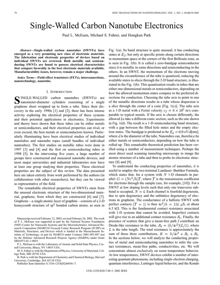
78 IEEE TRANSACTIONS ON NANOTECHNOLOGY, VOL. 1, NO. 1, MARCH 2002 Single-Walled Carbon Nanotube Electronics Paul L. McEuen, Michael S. Fuhrer, and Hongkun Park Abstract—Single-walled carbon nanotubes (SWNTs) have emerged as a very promising new class of electronic materials. The fabrication and electronic properties of devices based on individual SWNTs are reviewed. Both metallic and semiconducting SWNTs are found to possess electrical characteristics that compare favorably to the best electronic materials available. Manufacturability issues, however, remain a major challenge. Index Terms—Field-effect transistors (FETs), interconnections, nanotechnology, nanotube. I. INTRODUCTION S INGLE-WALLED carbon nanotubes (SWNTs) are nanometer-diameter cylinders consisting of a single graphene sheet wrapped up to form a tube. Since their discovery in the early 1990s [1] and [2], there has been intense activity exploring the electrical properties of these systems and their potential applications in electronics. Experiments and theory have shown that these tubes can be either metals or semiconductors, and their electrical properties can rival, or even exceed, the best metals or semiconductors known. Particularly illuminating have been electrical studies of individual nanotubes and nanotube ropes (small bundles of individual nantoubes). The first studies on metallic tubes were done in 1997 [3] and [4] and the first on semiconducting tubes in 1998 [5]. In the intervening five years, a large number of groups have constructed and measured nanotube devices, and most major universities and industrial laboratories now have at least one group studying their properties. These electrical properties are the subject of this review. The data presented here are taken entirely from work performed by the authors (in collaboration with other researchers), but they can be viewed as representative of the field. The remarkable electrical properties of SWNTs stem from the unusual electronic structure of the two-dimensional material, graphene, from which they are constructed [6] and [7]. Graphene—a single atomic layer of graphite—consists of a 2-D honeycomb structure of sp bonded carbon atoms, as seen in Manuscript received February 12, 2002; revised February 26, 2002. The work of P. L. McEuen was supported in part by the National Science Foundation (NSF) Center for Nanoscale Systems and the Microelectronics Advanced Research Corporation (MARCO) Focused Center Research Program (FCRP) on Materials, Structures, and Devices which is funded at the Massachusetts Institute of Technology, in part by MARCO under Contract 2001-MT-887 and by the Defense Advanced Research Projects Agency (DARPA) under Grant MDA972-01-1-0035. P. L. McEuen is with the Laboratory of Atomic and Solid State Physics, Cornell University, Ithaca, NY 14853 USA. M. S. Fuhrer is with the Department of Physics, University of Maryland, College Park, MD 20742 USA. H. Park is with the Department of Chemistry and Chemical Biology, Harvard University, Cambridge, MA 02138 USA. Publisher Item Identifier S 1536-125X(02)04581-7. Fig. 1(a). Its band structure is quite unusual; it has conducting , but only at specific points along certain directions states at in momentum space at the corners of the first Brillouin zone, as is seen in Fig. 1(b). It is called a zero-bandgap semiconductor since it is metallic in some directions and semiconducting in the others. In an SWNT, the momentum of the electrons moving around the circumference of the tube is quantized, reducing the available states to slices through the 2-D band structure, is illustrated in the Fig. 1(b). This quantization results in tubes that are either one-dimensional metals or semiconductors, depending on how the allowed momentum states compare to the preferred directions for conduction. Choosing the tube axis to point in one of the metallic directions results in a tube whose dispersion is a slice through the center of a cone [Fig. 1(c)]. The tube acts m/s comas a 1-D metal with a Fermi velocity parable to typical metals. If the axis is chosen differently, the allowed s take a different conic section, such as the one shown in Fig. 1(d). The result is a 1-D semiconducting band structure, with a gap between the filled hole states and the empty eleceV/d[nm], tron states. The bandgap is predicted to be where is the diameter of the tube. Nanotubes can, therefor,e be either metals or semiconductors, depending on how the tube is rolled up. This remarkable theoretical prediction has been verified using a number of measurement techniques. Perhaps the most direct used scanning tunneling microscopy to image the atomic structure of a tube and then to probe its electronic structure [8] and [9]. To understand the conducting properties of nanotubes, it is useful to employ the two-terminal Landauer–Buttiker Formula, 1-D channels in parwhich states that, for a system with , where is the transmission coefficient allel: for electrons through the sample (see, for example, [10]). For a SWNT at low doping levels such that only one transverse sub. Each channel is fourfold degenerate, band is occupied, due to spin degeneracy and the sublattice degeneracy of electrons in graphene. The conductance of a ballistic SWNT with is then S, or about perfect contacts 6.5 k . This is the fundamental contact resistance associated with 1-D systems that cannot be avoided. Imperfect contacts will give rise to an additional contact resistance . Finally, the presence of scatters that give a mean-free path contribute an , where Drude-like resistance to the tube, is the tube length. The total resistance is approximately the . sum of these three contributions, In the sections below, we will analyze the conducting properties of metal and semiconducting nanotubes to infer the contact resistances, mean-free paths, conductivities, etc. We will concentrate almost exclusively on room temperature behavior. At low temperatures, SWNT devices exhibit a number of interesting quantum phenomena, including single-electron charging, quantum interference, Luttinger liquid behavior, and the Kondo 1536-125X/02$17.00 © 2002 IEEE MCEUEN et al.: SWNT ELECTRONICS 79 Fig. 1. (a) Lattice structure of graphene, a honeycomb lattice of carbon atoms. (b) Energy of the conducting states as a function of the electron wavevector k . There are no conducting states except along special directions where cones of states exist. (c), (d) Graphene sheets rolled into tubes. This quantizes the allowed k s around the circumferential direction, resulting in 1-D slices through the 2-D band structure in (b). Depending on the way the tube is rolled up, the result can be either (c) a metal or (d) a semiconductor. effect, but these are not of direct relevance to most device applications. We, therefore, refer the reader to existing reviews for further discussion of these topics [11]–[13]. The critical issues with respect to device applications are twofold. The first is how reproducibly and reliably nanotube devices can be manufactured. Some current approaches to device fabrication are discussed in Section II. The second issue is how the electrical properties of SWNT devices compare to other electronic materials. These properties are described below in Sections III and IV for metallic and semiconducting tubes, respectively. These sections show that devices based on individual SWNTs have remarkable electrical characteristics, making them a very promising new class of electronic materials. The manufacturability challenges, however, are very significant. While advances are being made, controlled, reproducible device fabrication remains an unattained goal. These issues will be discussed in more detail in Section V. II. NANOTUBE GROWTH AND DEVICE FABRICATION SWNTs are grown by combining a source of carbon with a catalytic nanostructured material such as iron or cobalt at elevated temperatures. Sources of carbon employed to date include bulk graphite, hydrocarbons, and carbon monoxide. While the details of the growth process are far from understood, the basic elements are now coming into focus. A schematic is shown in Fig. 2(a). At elevated temperatures, the catalyst has a high solubility for carbon. The carbon in the particle links up to form graphene and wraps around the catalyst to from a cylinder. Subsequent growth occurs from the continuous addition of carbon to the base of the tube at the nanoparticle/tube interface. Remarkably, tubes can grow to lengths of hundreds of microns by this process [14]. Creating the proper conditions for growth can done in a variety of ways. From the point of view of device fabrication, the techniques can be divided into categories. In the first category are tubes grown by bulk synthesis techniques that are subsequently deposited on a substrate to make devices (“deposited tubes”). The most common methods for bulk fabrication are arc synthesis [1], [2] and laser assisted growth [15], and commercial sources of SWNTs from these techniques are now available. By controlling the growth conditions, high yields of SWNTs with narrow size distributions can be obtained. Unfortunately, tubes fabricated this way are in the form of a highly tangled “felt” of tubes and bundles of tubes. For electronic devices, these tubes 80 Fig. 2. (a) Schematic of a SWNT growing from a catalyst seed particle. (b) Atomic force microscope images of a single nanotube device fabricated using electron beam lithography. (c) Parallel fabrication of SWNT devices by growth from patterned catalysts and subsequent deposition of arrays of electrodes. The lower panel shows an AFM image of one pair electrodes bridged by two SWNTs. must be separated, cut into usable sizes, and then deposited on a substrate. This is typically done by ultrasonication in an appropriate solvent to disperse and cut the SWNTs, followed by deposition onto a substrate by spinning or drying. Unfortunately, this is to date an uncontrolled process, producing tubes on the substrate of varying lengths that are often still bundled together. This processing can also induce significant numbers of defects in the tubes. However, new techniques for the wet processing, cutting, and sorting of nanotubes are under constant development [16]–[20]. An alternative approach is to grow the nanotubes directly on the wafer [21]. Currently this is done using chemical vapor deposition (CVD). The catalyst material is placed on the surface of a wafer, which is inserted in a standard furnace at 700 C–1000 C in a flow of a carbon source gas such as methane. The tubes grow from the catalyst seeds on the substrate. Engineering the properties of the catalyst and controlling the growth conditions control the properties of the tubes. For example, relatively monodisperse nanoparticle catalysts have been shown to yield SWNTs with a diameter closely matching that of the catalyst particle [22] and [23]. For both deposited and CVD-grown SWNTs, the tubes must be integrated with electrodes and gates on a wafer to make devices. A major challenge is the placement of the tubes relative to lithographically patterned features on the substrate. For both CVD-grown and deposited tubes, techniques have been developed that are satisfactory for research purposes, if not for mass production. Examples are shown in Fig. 2. For the device in Fig. 2(b), SWNTs were grown by CVD and located relative to alignment marks on the surface using an atomic force microscope. Polymethylmethacrylate (PMMA) resist was then spun over the tubes and an electron beam mask was designed, followed by electron beam lithography and liftoff to attach the gold leads [4]. The tubes remain bound to the substrate are unaffected by standard solvents for resist patterning. An alternate approach [21] is to pattern arrays of small catalyst islands from which SWNTs are grown. Electrode arrays are then deposited over the IEEE TRANSACTIONS ON NANOTECHNOLOGY, VOL. 1, NO. 1, MARCH 2002 catalyst pads using optical or electron beam lithography. The result is pairs of electrodes with a random number of tubes connecting them, as seen in Fig. 2(c). By adjusting the parameters, a significant fraction of electrodes with only one tube bridging them can be obtained. Equivalent approaches exist to create devices for deposited tubes, with the CVD growth step replaced by a deposition step. An alternative method available for deposited tubes is to pattern the electrodes first and then deposit the tubes on top of the electrodes [3]. This avoids the high-temperature growth step, and chemical modification of the surface [24] and/or electric fields can be used to control, to some degree, the locations of the deposited tubes. A schematic of the resulting device geometry is shown in the inset to Fig. 5. Source and drain electrodes allow the conducting properties of the nanotube to be measured, and a third gate electrode gate is used to control the carrier density on the tube. Typically, the degenerately doped Si substrate is used as the gate. Nearby metal electrodes [3], an oxidized Al electrode under the tube [25], and even an ionic solution around the tube [26] and [27] have also been employed as gates. When the conductance of the tube as the gate voltage, and hence the charge per unit length of the tube, is varied is measured, two classes of behavior are seen. For some tubes, is relatively independent of , corresponding to a metallic tube. These are discussed in Section III. For other tubes, a dramatic dependence of on is seen, indicating semiconducting tubes. These will be discussed in Section IV. III. ELECTRICAL PROPERTIES OF METALLIC TUBES Devices made from metallic SWNTs were first measured in 1997 [3] and [4], and have been extensively studied since that time. Two-terminal conductances of metallic SWNTs at room temperature can vary significantly, ranging from as small as 6-k to several megaohms (M ). Most of this variation is due to variations in contact resistance between the electrodes and the tube. As techniques for making improved contacts have been developed, the conductances have steadily improved. The best contacts have been obtained by evaporating Au or Pt over the tube, often followed by a subsequent anneal. A number of groups have seen conductances approaching the value, , predicted for a ballistic nanotube [28] and [29]. An exas a function of ample is shown in Fig. 3, where the is shown for a 1- m long SWNT. At low , the conductance , growing to at the temperature is lowered. is Assuming perfect contacts, this indicates that the mean-free path is at least 1 m at room temperature and grows even larger as the device is cooled. A number of other measurements corroborate this conclusion, such as measurements of short tubes where is found [28] and [29], and scanned probe experiments that probe the local voltage drop along the length of the nanotube [30]. This mean-free path corresponds to a room temcm. The conductivity of metallic perature resistivity of nanotubes can, thus, be equal to, or even exceed, the conductivity of the best metals at room temperature. These long scattering lengths are in striking contrast to the behavior observed in traditional metals like copper, where scattering lengths are typically on the order of tens of nanometers MCEUEN et al.: SWNT ELECTRONICS Fig. 3. Differential conductance dI=dV of a metallic SWNT as a function of V , at different temperatures. The conductance at low V approaches the values for a ballistic SWNT, 4e2=h. At higher V , the conductance drops dramatically due to optic and zone-boundary phonon scattering. at room temperature, due to phonon scattering. The main difference is the significantly reduced phase space for scattering by acoustic phonons in a 1-D system. At room temperature, acoustic phonons have much less momentum than the electrons at the Fermi energy. In a traditional metal, phonons backscatter electrons through a series of small angle scattering events that eventually reverse the direction of an electron. This is not possible in a 1-D conductor such as a nanotube, where only forward and backward propagation is possible. Note that while the mean-free path is much larger than traditional metals, the conductivity is only comparable to slightly better. This is because the effective density of states in nanotubes is much lower than traditional metals because of the semimetallic nature of graphene. Optic and zone-boundary phonons have the necessary momentum to backscatter electrons in nanotubes. They are too high meV) to be present at room temperature in energy ( . At high source–drain voltages, however, electrons and low can emit these phonons and efficiently backscatter. This leads to a dramatic reduction of the conductance at high biases, as was first reported by Yao et al. [31]. This can be readily seen in , the data of Fig. 3. The scattering rate grows linearly with leading to a saturation of the total current through the tube. This A for small-diameter saturation value is SWNT. This corresponds to a current density of A/cm for a 1 nm diameter tube. This is orders of magnitude larger than current densities found in present-day interconnects. This large current density can be attributed to the strong covalent bonding of the atoms in the tube. Unlike in metals, there are no low energy defects, dislocations, etc., that can easily lead to the motion of atoms in the conductor. In addition to phonon scattering, scattering off of static disorder (defects, etc.) is also possible in metallic tubes. A number of sources of scattering have been identified, including physical bends in the tube [32] and [33] and localized electronic states created at defects along the tube [34]. One technique that can give direct information about these scattering centers is scanned gate microscopy (SGM). In this technique, a metallized AFM tip is used as a local gate to probe the conducting properties. Fig. 4 shows a SGM image of a metallic tube [34]. The dark features in the images correspond to locations of defects, which 81 Fig. 4. Left panel: AFM image of a metallic SWNT. Other panels: Scanned gate microscopy of defects in the SWNT at different AFM tip voltages. The conductance through the SWNT is recorded as a function of the tip position. Resonant scattering at defect sites is indicated by rings of reduced conductance (dark) centered on the defects. Fig. 5. Conductance G versus gate voltage V of a p-type semiconducting SWNT field effect transistor. The device geometry is shown schematically in the inset. are conjectured to be associated with a bond-rotation defect in the nanotube. Measurements show that these defects are more common in tubes grown at lower temperatures ( 700 C). With proper control of the growth parameters, however, static defects can be minimized so that they are not an important source of scattering at room temperature. IV. ELECTRICAL PROPERTIES OF SEMICONDUCTING TUBES Semiconducting behavior in nanotubes was first reported by Tans et al. in 1998 [5]. Fig. 5 shows a measurement of the conductance of a semiconducting SWNT as the gate voltage applied to the conducting substrate is varied. The tube conducts at negand turns off with a positive . The resistance change ative between the on and off state is many orders of magnitude. This device behavior is analogous to a p-type metal–oxide–semiconductor field-effect transistor (MOSFET), with the nanotube replacing Si as the semiconductor. At large positive gate voltages, n-type conductance is sometimes observed, especially in larger-diameter tubes [35] and [36]. The conductance in the n-type region is typically less than in the p-type region because of the work function of the Au electrodes. The Au Fermi level aligns with the valence band of the SWNT, making a p-type contact with a barrier for the injection of electrons. 82 Semiconducting nanotubes are typically p-type at because of the contacts and also because chemical species, particularly oxygen, adsorb on the tube and act as weak p-type dopants. Experiments have shown that changing a tube’s chemical environment can change this doping level—shifting the voltage at which the device turns on by a significant amount [37] and [38]. This has spurred interest in nanotubes as chemical sensors. Adsorbate doping can be a problem for reproducible device beis obhavior, however. In air, a large hysteresis in versus served, with threshold voltage shifts of many volts common. In addition, the threshold voltage is very sensitive to the processing history of the device—for example, heating or exposure to UV radiation drives off oxygen [39], lowering the p-doping level of the device. Controlling adsorbate doping is an important challenge to be addressed. Recent work by the group at IBM has taken important steps in this direction [40]. Controlled chemical doping of tubes, both p- and n-type, has been accomplished in a number of ways. N-type doping was first done using alkali metals that donate electrons to the tube. This has been used to create n-type transistors [38], [41], [42], p-n junctions [43], and p-n-p devices [44]. Alkalai metals are not air-stable, however, so other techniques are under development, such as using polymers for charge-transfer doping [45]. While these techniques are progressing rapidly, we will concentrate here on tubes with no additional doping (beyond uncontrolled doping by adsorbates) and the carriers induced by the gate. For simplicity, we will further focus on the p-type conducting regime to get a sense of the basic parameters that characterize electrical transport. In the data of Fig. 5, the conductance initially rises linearly with as additional holes are added to the nanotube. At higher gate voltages, the conductance stops increasing and instead is constant. This limiting conductance is due both to the tube and to the contact resistance between the metallic electrodes and to the tube. The value of this resistance can vary by orders of magnitude from device to device, but by annealing the contacts, on-state resistances of 20–50 k can be routinely obtained. In the regime where grows linear with , the properties of the device can be described by the Drude-type relation , where is the capacitance per unit is the threshold voltage, is the mobility. length of the tube, The capacitance per unit length of the tube can be estimated or obtained from other measurements [3], [4], [46]. Using this we can infer the mobility of the tube, . We find typical mobilities of 1000–10 000 cm /V s for CVD-grown tubes, with occasional devices having mobilities as high as 20 000 cm /V s. This is significantly higher than the values reported to date in deposited nanotubes [25], [40], [47], [48]. It is also higher than the mobilities in Si MOSFETs, indicating than SWNTs are a remarkably high-quality semiconducting material. As with metallic tubes, work has also been performed to investigate the nature of the scattering sites in nanotubes. Again, scanned probe techniques has been very useful. A scanned gate microscopy measurement is shown in Fig. 6(a). The tip was biased positively, to locally deplete the carriers (holes) underneath the tip. The bright spots in the image correspond to places where the AFM tip affected the conductance of the sample, producing a map of the barriers to conduction. This data shows that the con- IEEE TRANSACTIONS ON NANOTECHNOLOGY, VOL. 1, NO. 1, MARCH 2002 Fig. 6. (a) Scanned gate microscopy showing scattering sites in a p-type semiconducting SWNT. (b) Voltage drop along the length of the source–drain biased semiconducting SWNT, as determined by electric force microscopy. The slope of the voltage drop (dotted line) indicates a resistance per unit length of 9 k =m. ductance is limited by a series of potential barriers that the holes see as they traverse the tube. The barriers are likely due local inhomogeneities in the surface potential from adsorbed charges, etc., at or near the tube. At higher densities, however, little effect of the tip was seen, suggesting excellent transport properties. Electric force microscopy [49] can be used to directly probe the voltage drop along the length of the channel; the result is shown if Fig. 6(b). A linear voltage drop corresponding m is observed, implying a mean-free to a resistance of 9 k path of 0.7 m, comparable to the mean-free paths in metallic tubes. This result is consistent with the maximum conductances for 1- m long observed for semiconducting SWNTs ( tubes) and the high mobilities discussed above. In order to maximize device performance, the tube gate cashould be maximized. Most experiments to date pacitance have used gate oxide thicknesses of hundreds of millimicrons. More recently, researchers have investigated a number of ways to increase the gate coupling, such as using a very thin Al oxide gate [25] or using an electrolyte solution as a gate [26] and [27]. The latter is schematically shown in Fig. 7(a), with the resulting – curves at different s shown in Fig. 7(b). Standard FET and behavior is seen; the current initially rises linearly with then becomes constant in the saturation region. The nanotube exhibits excellent characteristics, with a maximum transconducA/V at V. Normalizing this tance, to the device width of 2 nm, this gives a transconductance per unit width of 10-mS/ m. This is significantly better than current-generation MOSFETs. The properties of semiconducting SWNTs given above are quite remarkable. Perhaps most surprising is the high mobilities obtained given the small channel width and the simplicity of the fabrication methods employed. This is largely due to the lack of surface states in these devices. As is well known from bulk semiconductors, surface states generally degrade the operating properties of the device, and controlling them is one of the key technological challenges to device miniaturization. A SWNT solves the surface state problem in an elegant fashion. First, it MCEUEN et al.: SWNT ELECTRONICS Fig. 7. I –V characteristics at different V s for a p-type SWNT FET utilizing an electrolyte gate. A schematic of the measurement geometry is also shown. begins with a 2-D material with no chemically reactive dangling bonds. It then rids itself of the problem of edges by using the topological trick of rolling itself into a cylinder—which has no edges. 83 Much more challenging is the issue of device manufacturability. Although a great deal of work has been done, the progress to date has been modest. For example, in tube synthesis, the diameter of the tubes can be controlled, but not the chirality. As a result, the tubes are a mixture of metal and semiconductors. In CVD, the general location for tube growth can be controlled by patterning the catalyst material, but the number of tubes and their orientation relative to the substrate are still not well defined. Furthermore, the high growth temperature (900 C) for CVD tubes is incompatible with many other standard Si processes. The alternative approach, depositing tubes on a substrate after growth, avoids this high temperature issue but suffers from the chirality and positioning limitations discussed above. Furthermore, the wet processing of the tubes may degrade their electrical properties. Efforts are underway to address these issues. For example, techniques to guide tubes to desired locations during growth or deposition using electric fields [55] and/or surface modification [24] are being explored, with some success. To date, there are no reliable, rapid, and reproducible approaches to creating complex arrays of nanotube devices. This manufacturing issue is by far the most significant impediment to using nanotubes in electronics applications. While there has been significant fanfare around “circuits” made with nanotubes, (see, e.g., the “Breakthrough of the Year” for 2001 in Science magazine), in reality the accomplishments to date are a far cry from anything that would impress a device engineer or circuit designer. However, there appear to be no fundamental barriers to the development of a technology. The science of nanotubes has come a long way in five years. With the involvement of the engineering community, perhaps the technology of nanotubes will see similar progress in the next five. ACKNOWLEDGMENT The authors would like thank their many collaborators at Cornell University, Ithaca, NY, Harvard University, Cambridge, MA, and at the University of California at Berkeley who participated in the work described here. V. CHALLENGES AND FUTURE PROSPECTS The above results show that single nanotube devices possess excellent properties. Metallic tubes have conductivities and current densities that meet or exceed the best metals, and semiconducting tubes have mobilities and transconductances that meet or exceed the best semiconductors. This clearly make them very promising candidates for electronic applications. Opportunities also exist for integrating nanotube electronics with other chemical, mechanical, or biological systems. For example, nanotube electronic devices function perfectly well under biological conditions (i.e., salty water) and have dimensions comparable to typical biomolecules (e.g., DNA, whose width is approximately 2 nm). This makes them an excellent candidate for electrical sensing of individual biomolecules. The are also a host of other device geometries beyond the simple wire and FET structures described above that are under exploration. Examples include the p-n and p-n-p devices mentioned previously [43] and [44], nanotube/nanotube junctions [50]–[52], and electromechanical devices [53] and [54]. REFERENCES [1] S. Iijima and T. Ichihashi, “Single-shell carbon nanotubes if 1-Nm diameter,” Nature, vol. 363, pp. 603–605, 1993. [2] D. S. Bethune, C. H. Kiang, M. S. Devries, G. Gorman, R. Savoy, J. Vazquez, and R. Beyers, “Cobalt-catalyzed growth of carbon nanotubes with single-atomic-layerwalls,” Nature, vol. 363, pp. 605–607, 1993. [3] S. J. Tans, M. H. Devoret, H. Dai, A. Thess, R. E. Smalley, L. J. Georliga, and C. Dekker, “Individual single-wall carbon nanotubes as quantum wires,” Nature, vol. 386, pp. 474–477, 1997. [4] M. Bockrath, D. H. Cobden, P. L. McEuen, N. G. Chopra, A. Zettl, A. Thess, and R. E. Smalley, “Single-electron transport in ropes of carbon nanotubes,” Science, vol. 275, pp. 1922–1925, 1997. [5] S. J. Tans, R. M. Verschueren, and C. Dekker, “Room temperature transistor based on a single carbon nanotube,” Nature, vol. 393, pp. 49–52, 1998. [6] N. Hamada, S. Sawada, and A. Oshiyama, “New one-dimensional conductors—Graphitic microtubules,” Phys. Rev. Lett., vol. 68, pp. 1579–1581, 1992. [7] R. Saito, M. Fujita, G. Dresselhaus, and M. S. Dresselhaus, “Electronic structure of chiral graphene tubules,” Appl. Phys. Lett., vol. 60, pp. 2204–2206, 1992. [8] T. W. Odom, H. Jin-Lin, P. Kim, and C. M. Lieber, “Atomic structure and electronic properties of single-walled carbon nanotubes,” Nature, vol. 391, pp. 62–64, 1998. 84 [9] J. W. G. Wildoer, L. C. Venema, A. G. Rinzler, R. E. Smalley, and C. Dekker, “Electronic structure of atomically resolved carbon nanotubes,” Nature, vol. 391, pp. 59–62, 1998. [10] S. Datta, Electronic Transport in Mesoscopic Systems. Cambridge, MA: Cambridge Univ. Press, 1995. [11] C. Dekker, “Carbon nanotubes as molecular quantum wires,” Physics Today, vol. 52, p. 22, 1999. [12] J. Nygard, D. H. Cobden, M. Bockrath, P. L. McEuen, and P. E. Lindelof, “Electrical transport measurements on single-walled carbon nanotubes,” Appl. Phys. A, Solids Surf., vol. A69, pp. 297–304, 1999. [13] Z. Yao, C. Dekker, and P. Avouris, “Electrical transport through single-wall carbon nanotubes,” in Topics in Applied Physics, M. S. Dresselhaus, G. Dresselhaus, and P. Avouris, Eds. Berlin, Germany: Springer-Verlag, 2001, vol. 80, pp. 147–171. [14] N. R. Franklin and H. Dai, “An enhanced CVD approach to extensive nanotube networks with directionality,” Adv. Mater., vol. 12, pp. 890–894, 2000. [15] A. Thess, R. Lee, P. Nikolaev, H. Dai, P. Petit, J. Robert, X. Chunhui, L. Young Hee, K. Seong Gon, A. G. Rinzler, D. T. Colbert, G. E. Scuseria, D. Tombnek, J. E. Fischer, and R. E. Smalley, “Crystalline ropes of metallic carbon nanotubes,” Science, vol. 273, pp. 483–487, 1996. [16] J. Liu, A. G. Rinzler, H. Dai, J. H. Hafner, R. K. Bradley, P. J. Boul, A. Lu, T. Iverson, K. Shelimov, C. B. Huffman, F. Rodriguez-Macias, Y.-S. Shon, T. R. Lee, D. T. Colbert, and R. E. Smalley, “Fullerene pipes,” Science, vol. 280, pp. 1253–1256, 1998. [17] J. Chen, M. A. Hamon, H. Hu, Y. Chen, A. M. Rao, P. C. Eklund, and R. C. Haddon, “Solution properties of single-walled carbon nanotubes,” Science, vol. 282, pp. 95–98, 1998. [18] E. T. Mickelson, C. B. Huffman, A. G. Rinzler, R. E. Smalley, R. H. Hauge, and J. L. Margrave, “Fluorination of single-wall carbon nanotubes,” Chem. Phys. Lett., vol. 296, pp. 188–194, 1998. [19] J. Chen, A. M. Rao, S. Lyuksyutov, M. E. Itkis, M. A. Hamon, H. Hu, R. W. Cohn, P. C. Eklund, D. T. Dolbert, R. E. Smalley, and R. C. Haddon, “Dissolution of full-length single-walled carbon nanotubes,” J. Phys. Chem. B, vol. 105, pp. 2525–2528, 2001. [20] S. Niyogi, H. Hu, M. A. Hamon, P. Bhowmik, B. Zhao, S. M. Rozenzhak, J. Chen, M. E. Itkis, M. S. Meier, and R. C. Haddon, “Chromatographic purification of soluble single-walled carbon nanotubes (s-SWNT’s),” J. Amer. Chem. Soc., vol. 123, pp. 733–734, 2001. [21] J. Kong, H. T. Soh, A. Cassell, C. F. Quate, and H. Dai, “Synthesis of single single-walled carbon nanotubes on patterned silicon wafers,” Nature, vol. 395, p. 878, 1998. [22] Y. Li, W. Kim, Y. Zhang, M. Rolandi, D. Wang, and H. Dai, “Growth of single-walled carbon nanotubes from discrete catalytic nanoparticles of various sizes,” J. Phys.Chem. B, vol. 105, p. 11 424, 2001. [23] C. L. Cheung, A. Kurtz, H. Park, and C. M. Lieber, “Diameter controlled synthesis of carbon nanotubes,” J. Phys. Chem. B, vol. 105, 2002, to be published. [24] J. Liu, M. J. Casavant, M. Cox, D. A. Walters, P. Boul, L. Wei, A. J. Rimberg, K. A. Smith, D. T. Colbert, and R. E. Smalley, “Controlled deposition of individual single-walled carbon nanotubes on chemically functionalized templates,” Chem. Phys. Lett., vol. 303, pp. 125–129, 1999. [25] A. Bachtold, P. Hadley, T. Nakanishi, and C. Dekker, “Logic circuits with carbon nanotube transistors,” Science, vol. 294, pp. 1317–1320, 2001. [26] M. Kruger, M. R. Buitelaar, T. Nussbaumer, C. Schonenberger, and L. Forro, “Electrochemical carbon nanotube field-effect transistor,” Appl. Phys. Lett., vol. 78, pp. 1291–1293, 2001. [27] S. Rosenblatt, Y. Yaish, J. Park, J. Gore, and P. L. McEuen, “High performance electrolyte gates carbon nanotube transistors,” . [28] L. Wenjie, M. Bockrath, D. Bozovic, J. H. Hafner, M. Tinkham, and P. Hongkun, “Fabry–Perot interference in a nanotube electron waveguide,” Nature, vol. 411, pp. 665–669, 2001. [29] J. Kong, E. Yenilmez, T. W. Tombler, W. Kim, H. Dai, R. B. Laughlin, L. Liu, C. S. Jayanthi, and S. Y. Wu, “Quantum interference and ballistic transmission in nanotube electron waveguides,” Phys. Rev. Lett., vol. 87, pp. 106 801/1–106 891/4, 2001. [30] A. Bachtold, M. S. Fuhrer, S. Plyasunov, M. Forero, E. H. Z. Anderson, Z. A. Zettl, and P. L. McEuen, “Scanned probe microscopy of electronic transport in carbon nanotubes,” Phys. Rev. Lett., vol. 84, pp. 6082–6085, 2000. [31] Z. Yao, C. L. Kane, and C. Dekker, “High-field electrical transport in single-wall carbon nanotubes,” Phys. Rev. Lett., vol. 84, pp. 2941–2944, 2000. IEEE TRANSACTIONS ON NANOTECHNOLOGY, VOL. 1, NO. 1, MARCH 2002 [32] H. W. C. Postma, M. de Jonge, and C. Dekker, “Electrical transport through carbon nanotube junctions created by mechanical manipulation,” Phys. Rev. B, Condens. Matter, vol. 62, pp. R10653–R10656, 2000. [33] D. Bozovic, M. Bockrath, J. H. Hafner, C. M. Lieber, P. Hongkun, and M. Tinkham, “Electronic properties of mechanically induced kinks in single-walled carbon nanotubes,” Appl. Phys. Lett., vol. 78, pp. 3693–3695, 2001. [34] M. Bockrath, L. Wenjie, D. Bozovic, J. H. Hafner, C. M. Lieber, M. Tinkham, and P. Hongkun, “Resonant electron scattering by defects in single-walled carbon nanotubes,” Science, vol. 291, pp. 283–285, 2001. [35] J. Park and P. L. McEuen, “Formation of a p-type quantum dot at the end of an n-type carbon nanotube,” Appl. Phys. Lett., vol. 79, pp. 1363–1365, 2001. [36] A. Javey, M. Shim, and H. Dai, “Electrical properties and devices of large-diameter single-walled carbon nanotubes,” Appl. Phys. Lett., vol. 80, p. 1064, 2002. [37] J. Kong, N. R. Franklin, C. Zhou, M. G. Chapline, S. Peng, K. Cho, and H. Dai, “Nanotube molecular wires as chemical sensors,” Science, vol. 287, p. 622, 2000. [38] V. Derycke, R. Martel, J. Appenzeller, and P. Avouris, “Carbon nanotube inter- and intramolecular logic gates,” Nano Lett., vol. 1, pp. 453–456, 2001. [39] R. J. Chen, N. R. Franklin, K. Jing, C. Jien, T. W. Tombler, Z. Yuegang, and D. Hongjie, “Molecular photodesorption from single-walled carbon nanotubes,” Appl. Phys. Lett., vol. 79, pp. 2258–2260, 2001. [40] R. Martel, V. Derycke, C. Lavoie, J. Appenzeller, K. K. Chan, J. Tersoff, and P. Avouris, “Ambipolar electrical transport in semiconducting single-wall carbon nanotubes,” Phys. Rev.Lett., vol. 87, p. 256 805, 2001. [41] M. Bockrath, J. Hone, A. Zettl, P. L. McEuen, A. G. Rinzler, and R. E. Smalley, “Chemical doping of individual semiconducting carbon-nanotube ropes,” Phys. Rev. B, Condens. Matter, vol. 61, pp. R10606–R10608, 2000. [42] J. Kong, C. Zhou, E. Yenilmez, and H. Dai, “Alkaline metal-doped n-type semiconducting nanotubes as quantum dots,” Appl. Phys. Lett., vol. 77, pp. 3977–3979, 2000. [43] C. Zhou, J. Kong, E. Yenilmez, and H. Dai, “Modulated chemical doping of individual carbon nanotubes,” Science, vol. 290, pp. 1552–1555, 2000. [44] J. Kong, J. Cao, and H. Dai, “Chemical profiling of single nanotubes: Intramolecular p–n–p junctions and on-tube single-electron transistors,” Appl. Phys. Lett., vol. 80, p. 73, 2002. [45] J. Kong and H. Dai, “Full and modulated chemical gating of individual carbon nanotubes by organic amine compounds,” J. Phys. Chem. B, vol. 105, p. 2890, 2001. [46] D. H. Cobden, M. Bockrath, P. L. McEuen, A. G. Rinzler, and R. E. Smalley, “Spin splitting and even–odd effects in carbon nanotubes,” Phys. Rev. Lett., vol. 81, pp. 681–684, 1998. [47] R. Martel, T. Schmidt, H. R. Shea, T. Hertel, and P. Avouris, “Single- and multi-wall carbon nanotube field-effect transistors,” Appl. Phys. Lett., vol. 73, pp. 2447–2479, 1998. [48] P. L. McEuen, M. Bockrath, D. H. Cobden, Y.-G. Yoon, and S, G. Louie, “Disorder, pseudospins, and backscattering in carbon nanotubes,” Phys. Rev. Lett., vol. 83, p. 5098, 1999. [49] A. Bachtold, M. S. Fuhrer, S. Plyasunov, M. Forero, E. H. Anderson, A. Zettl, and P. I. McEuen, “Scanned probe microscopy of electronic transport in carbon nanotubes,” Phys. Rev. Lett., vol. 84, pp. 6082–6085, 2000. [50] Z. Yao, H. W. C. Postma, L. Balents, and C. Dekker, “Carbon nanotube intramolecular junctions,” Nature, vol. 402, p. 273, 1999. [51] J. Lefebvre, R. D. Antonov, M. Radosavljevic, J. F. Lynch, M. Llaguno, and A. T. Johnson, “Single-wall carbon nanotube based devices,” Carbon, vol. 38, pp. 1745–1749, 2000. [52] M. S. Fuhrer, J. Nygård, L. Shih, M. Forero, Y.-G. Yoon, M. S. C. Mazzoni, H. J. Choi, J. Ihm, S. G. Louie, Z. A. Zettl, and P. L. McEuen, “Crossed nanotube junctions,” Science, vol. 288, pp. 494–497, 2000. [53] T. Rueckes, K. Kim, E. Joselevich, G. Y. Tseng, C. L. Cheung, and C. M. Lieber, “Carbon nanotube-based nonvolatile random access memory for molecular computing,” Science, vol. 289, pp. 94–97, 2000. [54] T. W. Tombler, Z. Chongwu, L. Alxseyev, K. Jing, D. Hongjie, L. Lei, C. S. Jayanthi, T. Meijie, and W. Shi-Yu, “Reversible electromechanical characteristics of carbon nanotubes under local-probe manipulation,” Nature, vol. 405, pp. 769–772, 2000. [55] Y. Zhang, A. Chang, J. Cao, Q. Wang, W. Kim, Y. Li, N. Morris, E. Yenilmez, J. Kong, and H. Dai, “Electric-field-directed growth of aligned single-walled carbon nanotubes,” Appl. Phys. Lett., vol. 79, pp. 3155–3157, 2001. MCEUEN et al.: SWNT ELECTRONICS Paul L. McEuen was born in Norman, OK, in 1963. He received the B.S. degree in engineering physics from the University of Oklahoma in 1985 and the Ph.D.degree in applied physics from Yale University, New Haven, CT, in 1991. He was a Postdoctoral Researcher at the Massachusetts Institute of Technology, Cambridge, before joining the University of California at Berkeley in 1992, where he was an Assistant Professor and later Associate Professor of physics and a researcher at LBNL. In 2001, he joined the faculty of Cornell University, Ithaca, NY, as a Professor of physics. His research examines the science and technology of nanostructures, and has included studies of nanotubes, quantum dots, and single molecules. He also develops advanced measurement techniques to probe nanometer-scale systems. Michael S. Fuhrer received the B.S. degree in physics from the University of Texas at Austin in 1990 and the Ph.D. degree in physics from the University of California at Berkeley in 1998. Since 2000, he has been an Assistant Professor of physics at the University of Maryland, College Park. His research interests lie in the electronic and electromechanical properties of nanostructures, including carbon nanotubes, nanowires, and new two-dimensional nanostructures. 85 Hongkun Park was born in Seoul, Korea, in 1967. He received the B.S. degree in chemistry from Seoul National University, Seoul, Korea, in 1990 and the Ph.D. degree in physical chemistry from Stanford University, Stanford, CA, in 1996. Since 1999, he has been with the Department of Chemistry and Chemical Biology at Harvard University, Cambridge, MA, as an Assistant Professor. His research interests lie in the physics and chemistry of nanostructured materials, specifically: 1) to study electrical properties of individual molecules, clusters, carbon nanotubes, and their arrays and 2) to develop synthetic schemes for transition–metal–oxide nanostructures and to study their electronic and magnetic properties.
