PSPICE Student 9.1 Tutorial
advertisement

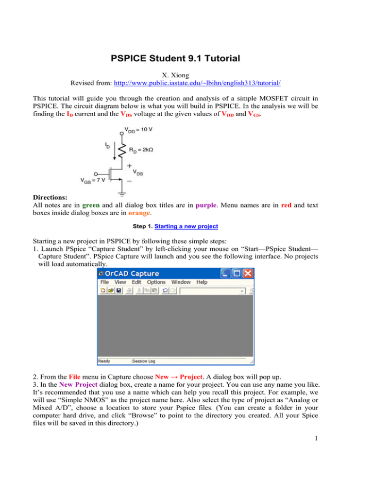
PSPICE Student 9.1 Tutorial X. Xiong Revised from: http://www.public.iastate.edu/~lbihn/english313/tutorial/ This tutorial will guide you through the creation and analysis of a simple MOSFET circuit in PSPICE. The circuit diagram below is what you will build in PSPICE. In the analysis we will be finding the ID current and the VDS voltage at the given values of VDD and VGS. Directions: All notes are in green and all dialog box titles are in purple. Menu names are in red and text boxes inside dialog boxes are in orange. Step 1. Starting a new project Starting a new project in PSPICE by following these simple steps: 1. Launch PSpice “Capture Student” by left-clicking your mouse on “Start—PSpice Student— Capture Student”. PSpice Capture will launch and you see the following interface. No projects will load automatically. 2. From the File menu in Capture choose New → Project. A dialog box will pop up. 3. In the New Project dialog box, create a name for your project. You can use any name you like. It’s recommended that you use a name which can help you recall this project. For example, we will use “Simple NMOS” as the project name here. Also select the type of project as “Analog or Mixed A/D”, choose a location to store your Pspice files. (You can create a folder in your computer hard drive, and click “Browse” to point to the directory you created. All your Spice files will be saved in this directory.) 1 4. After clicking OK, the Create PSPICE Project dialog box will pop up. It will ask you to choose which type of project you want to create. 5. Once you have clicked OK in the Create PSPICE Project dialog box, the schematic window will open and you are ready to begin adding libraries. Step 2. Adding libraries If you are using PSPICE for the first time on your computer or you are using a lab computer, the parts libraries will need to be added. Different libraries are needed for different types of circuits, so we will focus on the libraries containing the parts we need. 1. The first step in adding libraries can be done in one of two ways: a. Go to the Place menu and choose Part... b. From the icon bar on the right of the Capture window click the icon shown below. There are many useful icons in the right icon bar. Please point your mouse to each of these icons and the function of the pointed icon will be displayed. Please try to point all these icons separately to get familiar with them. They are short-cuts to menu paths and they can be very useful in our circuit design. For example, some useful icons include Select, Place part, Place wire, Place net alias, Place power, Place ground, Place off-page connector, etc. If the icon bar does not appear in the right side, just left click anywhere in the schematic window and the icon bar will appear. 2 2. The Place Part dialog box will appear and you will have the option to add libraries. 3. Library files have the extension .olb. If this type of file does not appear in the Browse File dialog box, in the Look in: drop down menu you will need to go to: C -> Program Files -> OrCAD_Demo -> Capture -> Library -> Pspice, After you have reached this location, the Browse File dialog box should look like the one below. 4. Please select all the available libraries: Left click on first library “abm”, then press your “shift” key and simultaneously click on the last library “special”, you will be able to select all the libraries as shown below. All the selected libraries will be in blue shade. Then click “Open”. 3 NOTE: We will only use a few libraries. 1). Analog and analog_p libraries: they are analog libraries. Actually they are very similar to each other. Analog contains analog parts such as resistor R, capacitor C, conductance L, etc. The different between the resistors in each library is very simple. The resistors in the analog_p library use a 1 and 2 at each end of the resistor to show the positive and negative ends of the resistor (1 for postive, 2 for negative). This isn't shown on the resistors in the analog library. 2). Breakout library: This includes MOS transistors (PMOS, NMOS), bi-polar transistor (NPN, PNP), etc. 3). Source library: This includes power sources, such as DC voltage Vdc, AC voltage Vac, Sin wave voltage VSIN, etc. 4. You will also need to add a library to use grounds in your circuit. Pspice must have this ground in order for proper simulation. Otherwise it will give error result. Select the Ground button from the icon bar on the right. 5. The Place Ground dialog box will look like the one below if you are using PSPICE for the first time on your computer or if you are using a lab computer. Once you choose the Add Library... button, go to the same location as we did above to add part libraries and add the source library. Please note that you only need to add library for the first time. In the future, you will not need to add the library anymore. Step 3. Inserting parts Now we will insert parts to construct our circuit. We design our circuit in 3 substeps: 1). First insert all the parts without considering their values (for example, the resistance value of a resistor, etc.). 4 2). After all the parts are inserted, we will make the necessary rotations for the parts, and move the parts to appropriate locations. 3). Then we will make all the necessary wire connections. 4). Finally, we will set the values for all the parts. In this circuit, we need to insert two DC voltage sources, one resistor, and one NMOS. 1. Get to the Place Part dialog box by using Place->Part from the menu or using the Place Part button on the icon bar. 2. All of the libraries will be highlighted. Click on the SOURCE library first in the Libraries box. In the Part List, scroll down to VDC and highlight it. The dialog box should look like the one below. 3. After clicking OK, you will be on the Schematic screen. Once you click the mouse on the Schematic screen, a DC voltage source will be inserted. Move the mouse and insert a second one. You should have something similar to what is shown below on your Schematic screen. After you finish placing two DC voltage source, you need to right click mouse and select (by left-click) “End mode”. Alternatively, you can just press the “Esc” key in your keyboard, then the red part in dotted rectangle will disappear. That is, you finish inserting the part of “DC voltage source”. Then you can continue to insert other parts or perform other operations. Note: If you placed extra DC voltage source, you can first right click to select “End mode”, then click “Select” icon on top right corner, then left click on the extra part to select it, and press “delete” key to delete it. You can also easily left click to select a part and drag it to anywhere in the schematic design. 5 4. Follow the procedure to get to the Place Part dialog box again. This time highlight ANALOG_P in the Libraries box and highlight r in the Part List box. The dialog box should look like the one below. 5. Click OK in the Place Part dialog box and then click once on the Schematic screen to insert a resistor. NOTE: Do not click more than once on the Schematic screen or you will have more than one resistor. 6. Go to the Place Part dialog box one more time. Highlight BREAKOUT in the Libraries box and highlight MbreakN3 in the Part List box. The dialog box should look like the one below. 6 7. After clicking OK, click only once on the Schematic screen because we only want to insert one NMOS. 8. Select the Place Ground button from the icon bar. In the Place Ground dialog box, highlight (left click to select) CAPSYM under Libraries and highlight GND under the Symbol box. Then left click on the “Name” bar to change the name from “GND” to “0”. You must change the name “GND” to “0” to indicate that this is the reference ground voltage (“0” node) of the circuit. Otherwise this “GND” node may stay at a voltage level other than 0V. Spice needs this “0” node in simulation. Otherwise it will cause error. The Place Ground dialog box should look like the one below. 9. Click OK and click once on the Schematic screen. Click “Select” icon in the right icon bar. On your Schematic screen you should have all of the parts shown below. 7 Step 4. Wiring the circuit The most difficult part of wiring the circuit is to make sure the polarity of the parts is correct. There are different ways to go about wiring the circuit, so feel free to try something different than what I show here. Just make sure that the direction of the sources in your schematic is the same as it is in mine. 1. First of all, you need to rotate some parts if it is required. For example, in our circuit we need to rotate resistor R1. In “Selecting” mode, left click to select (highlight) the resistor so a dashed line appears around the entire part. It should look like this: We need to rotate the resistor, which can be done in one of three ways. The easiest is to hold down CTRL and hit R. This will rotate the resistor 90 degrees. The second method is to select Rotate from the Edit menu. The last method is to right click on the resistor while it is highlighted and select Rotate. Rotate the resistor until it is vertical with the 1 at the top and the 2 at the bottom (3 rotations or 270 degrees). 2. Then you need to move the parts to appropriate locations in the schematic design. Click “Select” icon to enter “selecting” mode. Then left click on any part you want to move, and drag it to the right location and release the mouse button. This can move the part to anywhere in the design. For example, if the NMOS is the center of the circuit, you will want to position it between all of the parts. Also move the resistor to position it directly above the NMOS. 3. Now we are going to make all the wire connections. Select the Place Wire button from the icon bar or go the the Place menu and select Wire. You can left click your mouse on a point to start a wire in that point, then left click your mouse on another point to draw a wire to connect both points. If you don’t want more wires, right click your mouse to select “End wire”. If you draw extra wire connections, you can also select and delete them just like you select and delete extra parts. Use wire to connect the resistor and NMOS as shown below. 4. After all the wire connections are finished, now we are ready to set the values for all the parts. Select the numerical value of the resistor, labeled 1k (as shown below). Double-click on the numerical 8 value (1k) and the Display Properties dialog box will open. 1k will be displayed in the Value box. Change the value of “1k” to “2k” in the Value box of the Display Properties dialog box, as shown below. Note: If you wish, you can also change the name of the parts in a similar way. For example, if you wish to change the name of resistor R1 into “Rin”, you can double click on the name “R1” region, and the “Display Properties” interface will pop up. In the “Name: Part Reference” section, you can change the name from “R1” to “Rin”. However, this is just an example. Here we will still keep the name as “R1”. 6. Position all of your parts in a similar way to the one shown below. Pay attention to the upper voltage source's polarity as you rotate it. The + should be toward the resistor, not away from it. This will require three rotations. 9 7. Next connect the wires as we did above and follow the diagram below to connect the ground to the circuit. 8. We want to set the values of the V1 and V2 voltage sources to the values shown on the circuit diagram. The value of V1 is 7V and the value of V2 is 10V. Change these values exactly as we changed the resistor values. Double click on the voltage value and the “Display Properties” interface will pop up. Then you can change the voltage value. Before clicking OK in the Display Properties dialog box, be sure that the Vdc label is still after the number in the Value box. For example, V1 should be “7Vdc” instead of “7V” or “7”, as shown in following figure. 10 9. Now we can name some nodes which we are interested in. This is helpful if you wish to observe the voltage or current on these nodes. For example, we can name input and output nodes, etc. Here we wish to name the nodes of gate, drain and source of transistor M1 as Gm1, Dm1 and Sm1, separately. First left click on the “Place net alias” icon in right icon bar. The “Place Net Alias” interface will pop up. Input “Gm1” in “Alias” line, as shown below. Then click “OK”, and left click the node of the gate of transistor M1 (the node you wish to name it). Your net alias of “Gm1” will be placed. Repeat the similar process to name other nodes (drain and source of transistor M1 as Dm1 and Sm1 separately). Finally your design should look like: Step 5. Setting the parameters 11 As you have learned in class, the MOSFET has special parameters. The parameters we need to set are SPICE parameters for NMOS and PMOS, as well as the width (W) and length (L) of each transistor. We will learn how to set all of these parameters. Assume we need to set the size of MOS transistor M1 as W = 10µm, and L = 1µm. 1. First we will set the width (W) and length (L) of the MOS transistor M1. Highlight (Select) the NMOS in the same way we did to rotate parts in Step #4. That is, make sure the “Select” button on right panel is clicked, the left click on NMOS transistor to select (its color will change to red and a rectangle will surround it). Then right click on NMOS transistor and select “Edit Properties”. Alternatively, you can double-click on the NMOS and the Property Editor dialog box will open. 2. Left click on the scrolling bar on the bottom and drag it to the right until you see L in the first row. Click in the box underneath it, corresponding to the row labeled SCHEMATIC1:PAGE1:M1. Type 1e-6 in the box (for 1µm). Continue scrolling to the right until you see W in first row. Type 10e-6 in the box below (for 10µm). Your Property Editor box should look like the one below. Please note W is located at right most volumn. You may need to scroll the scrolling bar to the rightmost to see it. 12 NOTE: Before closing the Property Editor dialog box, be sure to click Apply. This will not close the dialog box, but it will ensure that the values you entered for the NMOS length and width are saved. After you have clicked Apply, you can use the X in the upper right hand corner to close the dialog box like you would close a program. 2. Now we are going to input the SPICE parameters for NMOS and PMOS transistor models. Highlight (left click to select it) the NMOS transistor, then Go to the Edit menu and select PSpice Model. The following dialog box will open. 13 3. Delete the line of: .model Mbreakn NMOS Then copy and paste following SPICE NMOS model parameter (You may also use other model parameters): * 1 um Level 3 models * * Don't forget the .options scale=1u if using an Lmin of 1 * 1<Ldrawn<200 10<Wdrawn<10000 Vdd=5V .MODEL Mbreakn NMOS LEVEL + TOX = 200E-10 + PHI = 0.7 + UO = 650 + KP = 120E-6 + RSH = 0 + XJ = 500E-9 + CGDO = 200E-12 + CJ = 400E-6 + CJSW = 300E-12 = 3 NSUB VTO ETA VMAX NFS LD CGSO PB = = = = = = = = 1E17 0.8 3.0E-6 1E5 1E12 100E-9 200E-12 1 GAMMA DELTA THETA KAPPA TPG = = = = = 0.5 3.0 0.1 0.3 1 CGBO MJ = 1E-10 = 0.5 MJSW = 0.5 Then press menu “File—Save” to save it. Be sure to save your model after you have saved, the asterisk after Mbreakn will disappear and your Model Editor dialog box will look like the one below. If you have a PMOS transistor Mbreakp in your design, you need to set the PMOS transistor SPICE model in a similar way, but copy and paste the following parameters for PMOS: 14 * 1 um Level 3 models * * Don't forget the .options scale=1u if using an Lmin of 1 * 1<Ldrawn<200 10<Wdrawn<10000 Vdd=5V .MODEL Mbreakp PMOS LEVEL + TOX = 200E-10 + PHI = 0.7 + UO = 250 + KP = 40E-6 + RSH = 0 + XJ = 500E-9 + CGDO = 200E-12 + CJ = 400E-6 + CJSW = 300E-12 = 3 NSUB VTO ETA VMAX NFS LD CGSO PB MJSW = = = = = = = = = 1E17 -0.9 0 5E4 1E12 100E-9 200E-12 1 0.5 GAMMA DELTA THETA KAPPA TPG = = = = = 0.6 0.1 0.1 1 -1 CGBO MJ = 1E-10 = 0.5 4. Once you have saved, close the Model Editor dialog box by choosing File -> Exit. The circuit is now created and the part parameters have been set. You're ready to move on!! Step 6. Running the analysis In this step, we will create a new PSPICE simulation and run the analysis. 1. Under the PSpice menu choose New Simulation Profile. The New Simulation dialog box will open up. In this box type a name for your simulation. It is good practice to use the same name for your simulation as you used for your project. 2. Click Create and the Simulation Settings dialog box will open. For our analysis, we want to do a Time Domain (Transient). All of the settings in the dialog box will be correct as long as the type of analysis is correct. In this simulation, we would like to set the total simulation time (TSTOP) to be 10ms, and the maximum step size as 0.01ms. We can change the settings and the Analysis tab of the Simulation Settings dialog box should look like the one below. 15 3. Click OK and you will return to the schematic. The next step is to run the simulation. This can be done by choosing Run from the PSpice menu, or by hitting F11, or by choosing the Play button from the icon bar at the top of the screen. 4. The PSPICE analysis window will open. Now you are ready to analyze the output file to determine the ID current and VDS voltage. Step 7. Analyzing the output file In the output file we will find the nodes necessary to make plots of the current and voltage. 1. In the PSPICE window, under View select Output File. This will display your output file. Scroll through the output file until you find a list similar to the following. 16 2. Under View choose Simulation Results. This will take you back to the screen where we can plot our values. Under Trace select Add Trace. The following window will open. 4. We want to view the current across the resistor. Generally, I(part_name) means the current flowing through the part_name, V(node_name) means the voltage level on the node_name. Click on I(R1) and it will appear in the Trace Expression box. This is the ID current (drain current of transistor M1). I(R1) is the current flowing through resistor R1. Select OK and we will return to the simulation results. In the simulation results screen, a straight light displaying the current will be plotted. 17 5. Now we will add one more plot of VDS voltage in the same window. Click on menu Plot—Add Plot to Window, a new blank plot will appear in the same window. Please note that VDS=V(Dm1)-V(Sm1), where Dm1 and Sm1 are the drain and source node names we defined before using “Place net alias” function. Under the Trace menu select Add Trace. In the Add Traces dialog box, first click on “V(Dm1)”, then click on the “-“ sign under “Analog Operations and Functions”, then click on “V(Sm1)”. Now “V(D1)-V(Sm1)” should appear in Trace Expression region. Click OK and you will return to the simulation results. 18 You should get following plots for “V(Dm1)-V(Sm1)” and “I(R1)”. 5. A straight line depicting the voltage has been displayed on the simulation results screen. To find exact numbers we return to the Capture window containing the schematic. 6. Under the PSpice menu in Capture, select Bias Points -> Enable Bias Current Display. Alternatively you can click on the icon of “Enable Bias Voltage Display” on the top icon bar, as shown below. The currents flowing through all parts will be displayed in red as shown below. The current through the resistor is approximately 4.250mA which is the ID current. 7. If you want to observe the exact values of all the node voltages, you can return to the PSpice menu and select Bias Points -> Enable Bias Voltage Display. Alternatively, you can click on 19 the icon of “Enable Bias Voltage Display” on the top icon bar, as shown below. The voltages on all the nodes will be displayed in maroon as shown below. We see that the VDS voltage is approximately equal to 1.501V. We have finished building the circuit, running it, and solving it. You can use different types of analyses to see when the NMOS changes regions. The best way to learn more about PSPICE is to try out its different functions. 20


