5 – 6 GHz 10 Watt Power Amplifier
advertisement
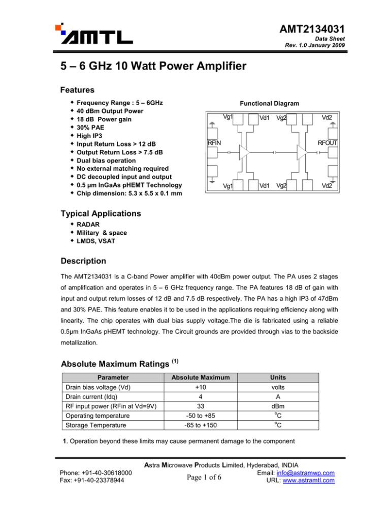
AMT2134031 Data Sheet Rev. 1.0 January 2009 5 – 6 GHz 10 Watt Power Amplifier Features Frequency Range : 5 – 6GHz 40 dBm Output Power 18 dB Power gain 30% PAE High IP3 Input Return Loss > 12 dB Output Return Loss > 7.5 dB Dual bias operation No external matching required DC decoupled input and output 0.5 µm InGaAs pHEMT Technology Chip dimension: 5.3 x 5.5 x 0.1 mm Functional Diagram Vg1 Vd1 Vg2 RFIN Vd2 RFOUT Vg1 Vd1 Vg2 Vd2 Typical Applications RADAR Military & space LMDS, VSAT Description The AMT2134031 is a C-band Power amplifier with 40dBm power output. The PA uses 2 stages of amplification and operates in 5 – 6 GHz frequency range. The PA features 18 dB of gain with input and output return losses of 12 dB and 7.5 dB respectively. The PA has a high IP3 of 47dBm and 30% PAE. This feature enables it to be used in the applications requiring efficiency along with linearity. The chip operates with dual bias supply voltage.The die is fabricated using a reliable 0.5µm InGaAs pHEMT technology. The Circuit grounds are provided through vias to the backside metallization. Absolute Maximum Ratings (1) Parameter Drain bias voltage (Vd) Drain current (Idq) RF input power (RFin at Vd=9V) Operating temperature Storage Temperature Absolute Maximum Units +10 4 33 volts A dBm -50 to +85 -65 to +150 o o C C 1. Operation beyond these limits may cause permanent damage to the component Astra Microwave Products Limited, Hyderabad, INDIA Phone: +91-40-30618000 Fax: +91-40-23378944 Page 1 of 6 Email: info@astramwp.com URL: www.astramtl.com AMT2134031 Data Sheet Rev. 1.0 January 2009 Electrical Specifications (1) @ TA = 25 oC, Vd1 = Vd2 = 9V, Vg1 = Vg2 = -0.9V Zo =50 Ω Parameter Typ. Units 5–6 GHz 18 dB +/-1.25 dB 39.5 dBm Input Return Loss 12 dB Output Return Loss 7.5 dB Saturated output power (Psat) 40.5 dBm 47 dBm 30% -- Supply Current(Idq) 2.9 A Supply Current (Idsat) 3.5 A Frequency Range Gain Gain Flatness Output Power (P1 dB) Output Third Order Intercept (IP3) Power Added Efficiency (PAE) Note: 1. TB – MMIC base temperature 2. Measured at output 1dB compression point 3. Operating current should be in between Idq and Idsat Astra Microwave Products Limited, Hyderabad, INDIA Phone: +91-40-30618000 Fax: +91-40-23378944 Page 2 of 6 Email: info@astramwp.com URL: www.astramtl.com AMT2134031 Data Sheet Rev. 1.0 January 2009 Test fixture data Vd1 = Vd2 = 9V, Vg1 = Vg2 = -0.9V, Total Current =2.9A, TA = 25 oC Gain 26 24 22 20 S21 [dB] 18 16 14 12 10 8 6 4 4.5 4.6 4.7 4.8 4.9 5 5.1 5.2 5.3 5.4 5.5 5.6 5.7 5.8 5.9 6 Frequency [GHz] Output P1dB and Psat 45 44 Psat & P1dB [dBm] 43 42 Psat 41 40 P1dB 39 38 37 36 35 5 5.1 5.2 5.3 5.4 5.5 5.6 Frequency [GHz] 5.7 5.8 5.9 6 Astra Microwave Products Limited, Hyderabad, INDIA Phone: +91-40-30618000 Fax: +91-40-23378944 Page 3 of 6 Email: info@astramwp.com URL: www.astramtl.com AMT2134031 Data Sheet Rev. 1.0 January 2009 Test fixture data Vd1 = Vd2 = 9V, Vg1 = Vg2 = -0.9V, Total Current =2.9A, TA = 25 oC Return Loss 0 -2 -4 S11 & S22 [dB] -6 S22 -8 S11 -10 -12 -14 -16 -18 -20 4.5 4.6 4.7 4.8 4.9 5 5.1 5.2 5.3 5.4 5.5 5.6 5.7 5.8 5.9 6 5.5 5.6 5.7 5.8 5.9 6 Frequency [GHz] Isolation -40 -45 S12 [dB] -50 -55 -60 -65 -70 4.5 4.6 4.7 4.8 4.9 5 5.1 5.2 5.3 5.4 Frequency [GHz] Astra Microwave Products Limited, Hyderabad, INDIA Phone: +91-40-30618000 Fax: +91-40-23378944 Page 4 of 6 Email: info@astramwp.com URL: www.astramtl.com AMT2134031 Data Sheet Rev. 1.0 January 2009 Bond Pad Locations 2 3 5 6 7 10 9 8 Units: millimeters (inches) Note: 1. All RF and DC bond pads are 100µm x 100µm 2. Pad no. 1 : RF IN 3. Pad no. 3 : 1st stage drain voltage(Vd1) 4. Pad no. 7 : RF Output 5. Pad no. 5,9 : 2nd stage drain voltage(Vd2) 6. Pad no. 10 : 2 nd stage gate voltage(Vg2) st 7. Pad no. 11 : 1 stage gate voltage (Vg1) Astra Microwave Products Limited, Hyderabad, INDIA Phone: +91-40-30618000 Fax: +91-40-23378944 Page 5 of 6 Email: info@astramwp.com URL: www.astramtl.com AMT2134031 Data Sheet Rev. 1.0 January 2009 Recommended Assembly Diagram Note : 1. 2. 3. 4. 5. 6. Two 1 mil (0.0254mm) bond wires of minimum length should be used for RF input and output. Two 1 mil (0.0254mm) bond wires of minimum length should be used from chip bond pad to 100pF capacitor. Input and output 50 ohm lines are on 5 mil RT Duroid substrate 0.1 µF capacitors may be additionally used as a second level of bypass for reliable operation The RF input & output ports are DC decoupled on-chip. Proper heat sink like Copper tungsten or copper molybdenum to be used for better reliability of chip Die attach: For Epoxy attachment, use of a two-component conductive epoxy is recommended. An epoxy fillet should be visible around the total die periphery. If Eutectic attachment is preferred, use of fluxless AuSn (80/20) 1-2 mil thick preform solder is recommended. Use of AuGe preform should be strictly avoided. Wire bonding: For DC pad connections use either ball or wedge bonds. For best RF performance, use of 150 - 200µm length of wedge bonds is advised. Single Ball bonds of 250-300µm though acceptable, may cause a deviation in RF performance. GaAs MMIC devices are susceptible to Electrostatic discharge. Proper precautions should be observed during handling, assembly & testing All information and Specifications are subject to change without prior notice Astra Microwave Products Limited, Hyderabad, INDIA Phone: +91-40-30618000 Fax: +91-40-23378944 Page 6 of 6 Email: info@astramwp.com URL: www.astramtl.com
