Molecular Dynamics and First-Principles Computations of Ga adlayers on GaN(0001) 1
advertisement

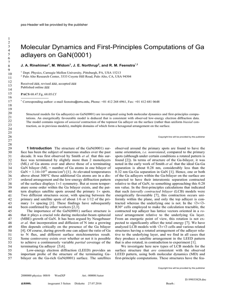
pss-Header will be provided by the publisher 1 2 3 4 5 6 7 8 9 10 11 12 13 14 15 16 17 18 19 20 21 22 23 24 25 26 27 28 29 30 31 32 33 34 35 36 37 38 39 40 41 42 43 44 45 46 47 48 49 50 51 52 53 54 55 56 57 Molecular Dynamics and First-Principles Computations of Ga adlayers on GaN(0001) J. A. Rinehimer1, M. Widom1, J. E. Northrup2, and R. M. Feenstra*,1 1 2 Dept. Physics, Carnegie Mellon University, Pittsburgh, PA, USA 15213 Palo Alto Research Center, 3333 Coyote Hill Road, Palo Alto, CA, USA 94304 Received zzz, revised zzz, accepted zzz Published online zzz PACS 68.47.Fg, 68.05.Cf * Corresponding author: e-mail feenstra@cmu.edu, Phone: +01 412 268 6961, Fax: +01 412 681 0648 Structural models for Ga adlayer(s) on GaN(0001) are investigated using both molecular dynamics and first-principles computations. An energetically favourable model is deduced that is consistent with observed low-energy electron diffraction data. The model contains regions of uniaxial contraction of the topmost Ga adlayer on the surface (rather than uniform biaxial contraction, as in previous models), multiple domains of which form a hexagonal arrangement on the surface. Copyright line will be provided by the publisher 1 Introduction The structure of the GaN(0001) surface has been the subject of numerous studies over the past decade. It was first observed by Smith et al. that this surface was terminated by slightly more than 2 monolayers (ML) of Ga atoms over and above those of a terminating GaN bilayer (ML = number of Ga atoms in one bilayer of GaN = 1.141015 atoms/cm2) [1]. At elevated temperatures above about 300C these additional Ga atoms are in a disordered arrangement and the low-energy diffraction pattern of the surface displays 11 symmetry. But at room temperature some order within the Ga bilayer exists, and the pattern displays satellite spots around the primary 1 spots. Two different structures occur, with spacing between the primary and satellite spots of about 1/6 or 1/12 of the primary 1 spacing [1]. These findings have subsequently been confirmed by other workers [2,3]. The importance of the GaN(0001) surface structure is that it plays a crucial role during molecular-beam epitaxial (MBE) growth of GaN. It has been argued by Neugebauer et al. that incorporation and diffusion of N into a growing film depends critically on the presence of the Ga bilayer [4]. Of course, during growth one can adjust the ratio of Ga to N flux, and different surface stoichiometries result. Some controversy exists over whether or not it is possible to achieve a continuously variable partial coverage of the terminating Ga adlayer [5,6]. Low-energy electron diffraction (LEED) provides an important probe of the structure of the terminating Gabilayer on the Ga-rich GaN(0001) surface. The satellites observed around the primary spots are found to have the same orientation, i.e. nonrotated, compared to the primary spots (although under certain conditions a rotated pattern is found [2]). In terms of structure of the Ga-bilayer, it was noted in the early work of Smith et al. that the ideal Ga-Ga separation is about 0.28 nm, considerably less than the 0.32 nm Ga-Ga separation in GaN [1]. Hence, one or both of the Ga adlayers within the Ga-bilayer on the surface are expected to have their interatomic separation contracted relative to that of GaN, to something approaching this 0.28 nm value. In the first-principles calculations that indicated that such laterally contracted bilayer (LCB) models were energetically favourable [7], this contraction occurs uniformly within the plane, and only the top adlayer is contracted whereas the underlying one is not. In the 33R30 cells employed to make the calculation tractable, the contracted top adlayer has lattice vectors oriented in a rotated arrangement relative to the underlying Ga layer. From an energetic point of view, this rotation is not expected to significantly affect the total energy [7]. We have analyzed LCB models with 33 cells and various related structures having a rotated arrangement of the adlayer relative to the underlying layer, and we find in all cases that they produce a satellite arrangement in the LEED pattern that is also rotated, in contradiction to experiment [1]. We investigate here new types of LCB models for the surface structure that are consistent with the observed LEED pattern, using both molecular dynamics (MD) and first-principle computations. These structures have the feaCopyright line will be provided by the publisher 2000000 physica 000/0 WordXP Art.: 00000/Autor D:\99033828.doc &R000; insgesamt 3 Seiten Diskette 27.07.2016 Bearb.: 2 1 2 3 4 5 6 7 8 9 10 11 12 13 14 15 16 17 18 19 20 21 22 23 24 25 26 27 28 29 30 31 32 33 34 35 36 37 38 39 40 41 42 43 44 45 46 47 48 49 50 51 52 53 54 55 56 57 ture of uniaxial (rather than uniform, biaxial) contraction of portions of a nonrotated top Ga adlayer, with equivalent domains of this structure all contributing to the final formation of a LEED pattern that agrees with experiment. 2 Theoretical MD simulations were carried out using the program “IMD” [8] with embedded-atom glue-type potentials for interatomic interactions. Reliable embeddedatom potentials for Ga are not available, while high-quality well-tested potentials are available for Al. We use a popular aluminum glue potential derived by a force-matching technique [9], and suitably scale our atomic structures to compensate for the differing atomic sizes of Ga and Al. The ideal Ga substrate spacing is a1x1 = 0.317 nm, while a laterally contracted adlayer having a 33 cell has average spacing (3/2) a1x1 = 0.275 nm, which is close to the natural spacing of Ga atoms that minimizes the energy of a free-standing bilayer of Ga [7]. We therefore adjust the substrate spacing to achieve lattice mismatch of 3/2 = 0.866 relative to the natural interatomic spacing of the adlayer atoms. Thus, although we employ an Al potential, the lattice mismatch between our substrate and adlayer is appropriate for the case of Ga on GaN(0001). In our simulations we fix the substrate atoms (i.e. the lower Ga adlayer) at their ideal positions and anneal the positions of upper adlayer atoms. We use a simulation cell of lateral dimensions 2747 nm and height 2.6 nm [10]. This cell contains a single layer of substrate atoms and approximately one layer of adatoms spaced initially at 0.24 0110 2110 Figure 1 Portion of an MD simulation for Ga coverage of 4/3 ML. Substrate atoms are shown by solid dots, adlayer atoms on the substrate are shown by open circle, and additional adatoms on top of the adlayer are shown by crosses. The inset shows a computed LEED pattern for this structure, extending over an area of 0.620.60 nm-2, showing a first-order primary spot and satellite spots around that. Copyright line will be provided by the publisher Author, Author, and Author: Short title nm from the substrate. The 2.6 nm cell height is sufficiently large to remove any influence of the periodic boundary conditions. As an initial condition we place the adlayer atoms in a regular triangular lattice. We then heat up to two times the bulk melting point and cool back down to low temperature, over a time of approximately 2 picoseconds. Diffusion and structural rearrangement is prevalent at the high temperature. LEED patterns were simulated in a straightforward manner by computing the structure factor of the adlayer plus substrate with a constraint on the wavevector that the kinetic energy of the electrons is 100 eV (as in the experiment [1]). Gaussian smoothing of the obtained pattern was performed over an interval of width 0.24 nm-1, and the contour plot shown here was made using the logarithm of the diffraction intensity. First-principle computations are performed using pseudopotential density functional theory, as discussed elsewhere [7]. The purpose of the calculation was to test whether a structure having a uniaxial contraction made sense from an energetic point of view. For this purpose a 16 cell was employed, with a contraction along the 6 direction. 3 Results and discussion Figure 1 shows the result of MD simulation with Ga coverage of 4/3 ML. We see that the adlayer forms a hexagonal arrangement on the substrate, with unit cells having typical size of 66. A few of the adatoms are found to be bonded on top of the adlayer. A computed LEED pattern is shown in the inset of Fig. 1. We find three satellite peaks, with spacing and orientation (i.e. nonrotated relative to the primary peaks) in agreement with “1/6” structure seen in experiment [1]. MD simulations have also been performed for coverages of 7/6 and 3/2 ML. The basic structure of the adlayer is found to be the same as in Fig. 1, although at 7/6 ML, vacancy islands appear in the adlayer whereas at 3/2 ML, islands of adatoms form on top of the adlayer. The hexagons apparent in Fig. 1 are composed of triangular regions, the edges of which are made of double or triple rows of atoms in which the spacing of the adlayer rows is less than that of the substrate. Along the horizontal [2110] direction in the figure the adlayer atoms are seen to have equal spacing as the substrate atoms, whereas along the vertical [0110] direction the spacing of the adlayer rows is significantly less than that of the substrate rows. In other words, the adlayer atoms here are uniaxially contracted relative to the substrate atoms. This appearance of uniaxial contraction in the surface structure is an interesting prediction of the MD simulation. To further investigate this feature we have performed firstprinciple computations on a model with 7/6 coverage of the top Ga adlayer, as shown in Fig. 2. The structure has a 16 unit cell as shown, and contains two adlayers of Ga atoms. The lower adlayer has Ga density identical with that of GaN, with the Ga atoms in this adlayer residing almost directly above the underlying Ga atoms of the underlying pss-Header will be provided by the publisher 1 2 3 4 5 6 7 8 9 10 11 12 13 14 15 16 17 18 19 20 21 22 23 24 25 26 27 28 29 30 31 32 33 34 35 36 37 38 39 40 41 42 43 44 45 46 47 48 49 50 51 52 53 54 55 56 57 GaN bilayer. The upper adlayer contains 7 Ga atoms in each unit cell; the Ga-Ga separation along the 6 direction is thus contracted [uniaxially, along the [1120] direction in Fig. 2(b)] relative to the underlying Ga layer. The separation of the lower adlayer from the underlying bilayer is about 0.249 nm. The separation between the two adlayers is about 0.241 nm, with a vertical corrugation in the upper adlayer of 0.016 nm arising from the varying registry of those Ga atoms with ones in the lower adlayer. The contraction of the upper Ga adlayer is expected to produce satellite spots around the primary LEED spots. A schematic view of the expected LEED pattern is shown in Fig. 2(c). There are three equivalent domains of the structure shown in Fig. 2 at 120 rotations, plus another three domains formed by a mirror reflection. These latter differ from the former only in terms of the nitrogen-atom positions in the 4th layer below the surface. The resulting energy difference is very small and so a typical multi-domain surface would be expected to contain all six of the orientations. The resulting LEED pattern would then appear as pictured in Fig. 2(d), which is again in agreement with the 3 “1/6” experimental result [1]. The total energy for the 16 Ga-bilayer shown in Fig. 2 is found to be within ~0.04 eV per 11 unit cell of that for the 33 model, in the Ga-rich limit. Regarding a complete model for the surface structure, one could visualize that as composed of many domains of 16 structure, assembled in a manner similar to that seen in the MD simulations. 4 Conclusion On the basis of both MD simulations and first-principles computations we have proposed a model for the structure of the Ga-rich GaN(0001) surface that yields a LEED pattern in agreement with experiment. This model consists of multiple-domains of uniaxially contracted bilayers on the surface, with strips of such regions forming a hexagonal type arrangement on the surface. The energy of a single 16 uniaxially compressed domain of this model is similar to LCB models with 33 cells, but it is expected that the energy of a larger domain structure (approximately 66) will yield lower energies. We have performed MD simulations at other values of the mismatch between adlayer and substrate (namely, 0.908, 0.914 and 0.920), yielding similar results to those described here although with larger hexagonal surface unit cells. The present model provides a feasible structure for the observed "1/6" structure of the Ga bilayer on GaN(0001), although the "1/12" surface is not yet explained and remains a topic for future research as does the surface structure of Al on AlN(0001) for which the observed LEED pattern has a rotated arrangement [11]. Acknowledgements We are grateful to P. Ganesh for useful discussions. This work was supported in part by the National Science Foundation, grant DMR-0503748. References Figure 2 (a) Side view, and (b) top view of the 16 model of the Ga-rich GaN(0001) surface. A 16 unit cell is shown in (b) by the dotted lines. In (b) the two Ga adlayers are shown, with the topmost Ga layer as dots and the lower Ga adlayer as open circles. (c) Single domain, and (d) multi-domain schematic LEED patterns, showing zeroth- and first-order spots, and satellites. www.pss-a.com [1] A. R. Smith, R. M. Feenstra, D. W. Greve, M.-S. Shin, M. Skowronski, J. Neugebauer, and J. Northrup, J. Vac. Sci. Technol B 16, 2242 (1998). [2] A. Pavlovska and E. Bauer, Surf. Sci. 480, 128 (2001). [3] C. Adelmann, J. Brault, G. Mula, B. Daudin, L. Lymperakis, and J. Neugebauer, Phys. Rev. B 67, 165419 (2003). [4] J. Neugebauer, T. K. Zywietz, M. Scheffler, J. E. Northrup, H. Chen, and R. M. Feenstra, Phys. Rev. Lett. 90, 056101 (2003). [5] C. Adelmann, J. Brault, D. Jalabert, P. Gentile, H. Mariette, G. Mula, and B. Daudin, J. Appl. Phys. 91, 9638 (2002). [6] J. S. Brown, G. Koblmüller, F. Wu, R. Averback, H. Riechert, and J. S. Speck, J. Appl. Phys. 99, 074902 (2006). [7] J. E. Northrup, J. Neugebauer, R. M. Feenstra, A. R. Smith, Phys. Rev. B 61, 9932 (2000). [8] J. Stadler, R. Mikulla, and H.-R. Trebin, Int. J. Mod. Phys. C 8, 1131-1140 (1997). [9] F. Ercolessi and J. B. Adams, Europhys. Lett. 26, 583 (1994). [10] All numerical values have been rescaled to correspond to Ga on GaN(0001). [11] C. D. Lee, R. M. Feenstra, J. E. Northrup, J. Neugebauer, Phys. Rev. B 68, 205317 (2003). Copyright line will be provided by the publisher


