APS-2 Single Pixel Test 7 February 2008
advertisement

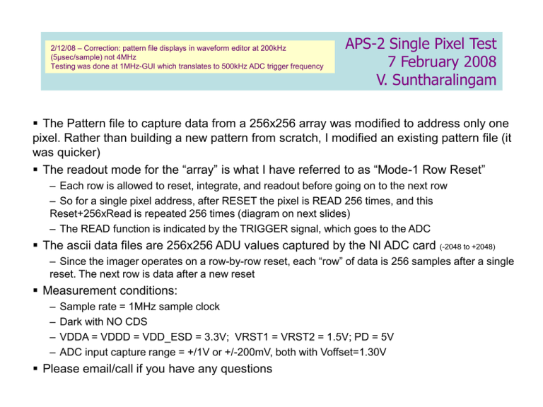
2/12/08 – Correction: pattern file displays in waveform editor at 200kHz (5µsec/sample) not 4MHz Testing was done at 1MHz-GUI which translates to 500kHz ADC trigger frequency APS-2 Single Pixel Test 7 February 2008 V. Suntharalingam The Pattern file to capture data from a 256x256 array was modified to address only one pixel. Rather than building a new pattern from scratch, I modified an existing pattern file (it was quicker) The readout mode for the “array” is what I have referred to as “Mode-1 Row Reset” – Each row is allowed to reset, integrate, and readout before going on to the next row – So for a single pixel address, after RESET the pixel is READ 256 times, and this Reset+256xRead is repeated 256 times (diagram on next slides) – The READ function is indicated by the TRIGGER signal, which goes to the ADC The ascii data files are 256x256 ADU values captured by the NI ADC card (-2048 to +2048) – Since the imager operates on a row-by-row reset, each “row” of data is 256 samples after a single reset. The next row is data after a new reset Measurement conditions: – – – – Sample rate = 1MHz sample clock Dark with NO CDS VDDA = VDDD = VDD_ESD = 3.3V; VRST1 = VRST2 = 1.5V; PD = 5V ADC input capture range = +/1V or +/-200mV, both with Voffset=1.30V Please email/call if you have any questions General Timing Diagram – Mode 1 (1) Address only Pixel r95c159: 65.5k times in cycle (RESET, READ) Timescale Here is for 200kHz sample clock Data taken with 1MHz sample clock Column Sample/Hold pulsing Trigger for ADC capture RSTG1 pulsing RSTG2 pulsing (2) Like previous, but Column SHS always ON Timescale Here is for 200kHz sample clock Data taken with 1MHz sample clock Ignore this display artifact Column Sample/Hold always conducting (to see if it contributes noise) RSTG1 pulsing RSTG2 pulsing (3a) Like first, but RSTG1 ON to fix first stage to DC level of VRST1 Timescale Here is for 200kHz sample clock Data taken with 1MHz sample clock Column Sample/Hold pulsing RSTG1 LOW RSTG2 pulsing Holds first stage to VRST1 (3b) Timescale Magnification: Pixel is read 256x after RSTG2 and SHS Timescale Here is for 200kHz sample clock Data taken with 1MHz sample clock SHS asserted for each “Row”, ADC Triggered 256x after each RESET This waveform helps us evaluate how long the charge is held on the SHS capacitor (4a) Like first, but Colmn SHS always on and RSTG1 always ON Timescale Here is for 200kHz sample clock Data taken with 1MHz sample clock Column Sample/Hold always conducting (to see if it contributes noise) RSTG1 LOW RSTG2 pulsing Holds first stage to VRST1 (4b) Timescale Magnification: Pixel is read 256x after RSTG2 Timescale Here is for 200kHz sample clock Data taken with 1MHz sample clock SHS always HIGH, ADC Triggered 256x after each RESET Data Files • Like slide #3, condition (1) • • w3r2c3_pixr95c159_m1_1M_RST15_PD5_voff130_1Vivr_dark.txt w3r2c3_pixr95c159_m1_1M_RST15_PD5_voff130_200mVivr_dark.txt • Like slides #5-6, condition (3) • • w3r2c3_pixr95c159_m1RG1Low_1M_RST15_PD5_voff130_1Vivr_dark.txt w3r2c3_pixr95c159_m1RG1Low_1M_RST15_PD5_voff130_200mVivr_dark.txt • Like slides #7-8, condition (4) • • w3r2c3_pixr95c159_m1RG1LowSHSHigh_1M_RST15_PD5_voff130_1Vivr_dark.txt w3r2c3_pixr95c159_m1RG1LowSHSHigh_1M_RST15_PD5_voff130_200mVivr_dark.txt +/-1V ADC Input capture range 1 ADU = 2/4096 +/-200mV ADC Input capture range 1 ADU = 0.4/4096


