Lab9
advertisement
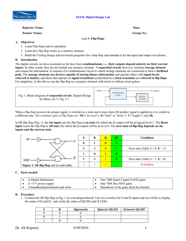
ES210, Digital Design Lab Reporter Name: Date: Partner Names Group No.: Lab 9: Flip-Flops A. Objectives 1. Learn Flip-flops and its operation. 2. Learn how flip-flop works as a memory element. 3. Build the Verilog design and test bench programs for a flop-flop and simulate it for the input and output waveforms. B. Introduction The digital circuits we have examined so far have been combinational, i.e., their outputs depend entirely on their current inputs. In other words, they do not include any memory element. A sequential circuit, however, includes storage element and retains the information. It consists of a combinational circuit to which storage elements are connected to form a feedback path. The storage elements are devices capable of storing binary information and operate either with signal levels referred to latches, and those that operate on signal transitions (controlled by a clock transition are referred to flip-flops. For simplicity, in this lab we use the flip-flop as a memory element with clock or without clock pulses. Fig. 1. Block diagram of sequential circuit, Digital Design by Mano, ed. 5, Fig. 5.1. When a flip-flop receives the proper signal, it switches to a state and it stays there till another signal is applied to it to switch to a different sate. The common types of flip-flops are: SR ("set-reset"), D ("data" or "delay"), T ("toggle"), and JK. In SR flip-flop (Fig. 1), the Set input sets the flip-flop to on state for which the Q output will be at logical level 1. The Reset input resets the flip-flop to off state for which the Q output will be at level 0. The next state of flip-flop depends on the inputs and the current state. Figure 1. SR flip-flop and its truth table. S R Q Q’ 0 1 0 1 0 0 0 1 1 0 1 0 0 0 1 0 Next state (After S = 1, R = 0) 1 1 1 1 Forbidden Condition Next state (After S = 0, R = 1) C. Parts needed A Digital Multimeter A +5 V power supply A breadboard/protoboard and wires One 7400 Quad 2-input NAND gates One 7404 Hex NOT gates Datasheets of the gates from the Internet D. Procedure 1. Connect the SR flip-flop in Fig. 1 on a bread/proroboard. Use two switches for S and R inputs and two LEDa to display the status of Q and Q’, and verify the states of QLEDs and Q’LEDs. S 0 0 1 Dr. Ali Kujoory R 0 1 0 Q(present) 0 0 0 6/30/2016 Q(next)=QLED Q'(next)=QLED’ 1 1 0 0 1 1 1 0 1 0 1 0 1 1 1 1 How about S=R=1, explain! Are Q and Q’ complementary? 2. Design a SR flip-flop with an En input to enable the device, i.e., when En=“1”, S and R signals can affect the state of the flip-flop and when En=”0”, S and R signal cannot affect the flip-flop state. (Hint: substitute each NOT gate with a NAND gate with the En input applied to both NAND gates. Draw the diagram in your logbook and show it to the instructor. Keep the circuit for next section. 3. Connect the circuit with a switch for the En input and 2 LEDs for Q and Q’ outputs. Complete the table below and verify the result. S 0 1 1 0 0 1 1 R 1 0 1 0 1 0 1 En 0 0 0 1 1 1 1 Q(present) 0 0 0 1 1 1 1 Q(next)=LED Q'(next)=QLED’ 4. D flip-flop is obtained from SR flip-flop with D=S=R’ as in Fig. 2. This avoids applying R=S=1 (indeterminate) to the SR flip-flop. The Enable input is replaced by a CK (clock) input, so the flip-flop can operate when the clock is high. From the truth table, D flip-flop simply can operate when the clock is high. D flip-flop is used in memory applications to store the data. Ck = En D Next State of Q 0 0 0 1 1 0 Q=0, Reset State 1 1 Q=1, Set State Q_LED No change Figure 2 D flip-flop and its truth table. (Mano, Fig 5.6). Construct the circuit in Fig. 2 on a bread/proroboard. Use a switch for D input and another switch to mimic the clock signal, one LED for the Q output to verify the operation of D-flip-flop. Explain and record the state of LED in the table. 5. To simulate the above circuit write a Verilog design program, called “D_flip_flop.v”, in the table below. Use “assign” keyword for all gates and w0, w1, w2, w3, etc., for the wires. Compile it to ensure it is error-free. 6. Then, write the corresponding Verilog test bench program in the table below. Include all the 4 combinations for D and CK with 50 ms delay between each combination entry in the program and a display span of 200 ms. Compile the program to ensure it is error-free. 7. Simulate the program to display the waveforms of the inputs D and CK and output Q and copy the display in the table below. Show your programs and displays to the instructor. Each member should present her and his Verilog portion. Dr. Ali Kujoory 6/30/2016 2 // D_flip_flop.v program module with all”assign” 15% // D_flip_flop_tb.v program module 15% Waveforms of inputs and outputs 10% E. Feedback/Comments (your comments will help improving this lab) Was the instruction clear enough? Any error? How difficult was it for you? Do you have any observations to make? F. Report 1. Report the answers you obtained and the display of waveforms in the tables above. You do not need to include the unnecessary text such as the objectives, instructions, and procedures in the report. 2. Each member should submit her/his Verilog section in the report with your name to make sure that every one exercises the Verilog program separately. (*) The author acknowledges Mr. S. Marivani and as some of the sections come from his work. Reference is made also to Wikipedia. Dr. Ali Kujoory 6/30/2016 3
