ENEE312H Spring 2002 Homework 3
advertisement
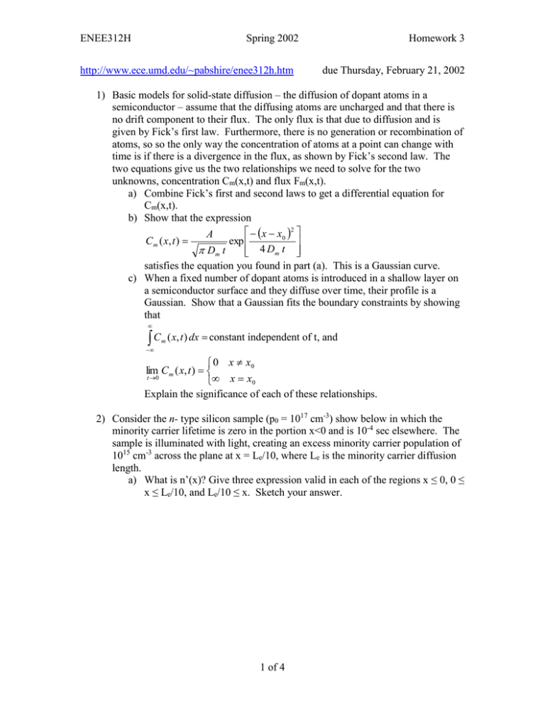
ENEE312H Spring 2002 http://www.ece.umd.edu/~pabshire/enee312h.htm Homework 3 due Thursday, February 21, 2002 1) Basic models for solid-state diffusion – the diffusion of dopant atoms in a semiconductor – assume that the diffusing atoms are uncharged and that there is no drift component to their flux. The only flux is that due to diffusion and is given by Fick’s first law. Furthermore, there is no generation or recombination of atoms, so so the only way the concentration of atoms at a point can change with time is if there is a divergence in the flux, as shown by Fick’s second law. The two equations give us the two relationships we need to solve for the two unknowns, concentration Cm(x,t) and flux Fm(x,t). a) Combine Fick’s first and second laws to get a differential equation for Cm(x,t). b) Show that the expression x x 0 2 A C m ( x, t ) exp Dm t 4 Dm t satisfies the equation you found in part (a). This is a Gaussian curve. c) When a fixed number of dopant atoms is introduced in a shallow layer on a semiconductor surface and they diffuse over time, their profile is a Gaussian. Show that a Gaussian fits the boundary constraints by showing that C m ( x, t ) dx constant independent of t, and 0 x x0 lim C m ( x, t ) t 0 x x0 Explain the significance of each of these relationships. 2) Consider the n- type silicon sample (p0 = 1017 cm-3) show below in which the minority carrier lifetime is zero in the portion x<0 and is 10-4 sec elsewhere. The sample is illuminated with light, creating an excess minority carrier population of 1015 cm-3 across the plane at x = Le/10, where Le is the minority carrier diffusion length. a) What is n’(x)? Give three expression valid in each of the regions x ≤ 0, 0 ≤ x ≤ Le/10, and Le/10 ≤ x. Sketch your answer. 1 of 4 ENEE312H Spring 2002 Homework 3 b) What is the optical hole-pair generation rate in the plane x = Le/10? 3) It is very difficult to maintain charge imbalances for long times or over long distances in an extrinsic semiconductor, so the material tends to stay electrically neutral (we call it quasineutral). The relevant time factor is the dielectric time constant; the relevant distance factor is the Debye length. a) A macroscopic example of dielectric relaxation is the decay of charge stored on a “leaky” capacitor. Such a capacitor might be a parallel plate capacitor with a conducting dielectric (i.e., one with dielectric constant and nonzero conductance ). A leaky capacitor can be modeled as an ideal capacitor in parallel with an ideal resistor. i. Show that the charge stored on a capacitor of capacitance C in parallel with resistance R will decay as t Q(t ) Q0 e RC if the charge at t=0 is Q0 . ii. Find an expression for the resistance R of a leaky capacitance with plate area A and plate separation d. iii. Find an expression for the capacitance C of the same capacitor. iv. Find an expression for the RC time constant of this leaky capacitor. This is the dielectric relaxation time. b) Calculate the dielectric relaxation time of the following materials: i. A metal with = 106 ( cm)-1, and = 10-13 C/(V cm) ii. An insulator with = 10-16 ( cm)-1, and = 3x10-13 C/(V cm) iii. A semiconductor with = 100 ( cm)-1, and = 10-12 C/(V cm) 4) Consider three different silicon samples: an n- sample with Nd = 5x1015 cm-3, an n+- sample with Nd = 1018 cm-3, and a p- sample with Na = 1017 cm-3. a) Following the convention that 0 in intrinsic material, what is in each of these samples at room temperature? b) Calculate the built-in voltage b of a junction (i) between the p- and nsamples and (ii) between the p- and n+- samples. c) Derive an expression for the electrostatic potential difference between two uniformly doped n- type regions. Use this expression to calculate the potential difference (built-in potential) between the n- and n+- samples. 2 of 4 ENEE312H Spring 2002 Homework 3 d) The electrostatic potential of a certain metal relative to intrinsic silicon is 0.05 V at room temperature. What is the contact potential between this metal and (i) the n+- sample? (ii) the p- sample? e) Use your answers from parts (a) through (d) to show that the change in electrostatic potential going around the circuit shown in the figure below is zero. 5) An important variant on the abrupt p-n junction is the p-i-n diode, where i stands for intrinsic. An example is shown in the figure below. The idea is that the largest fields and most of the voltage drop occur across the intrinsic region. In this problem use wn = wp = 2 m and wi = 1 m. Also assume that T=27ºC (300K) and ni = 1010 cm-3. a) What is the electrostatic potential on the n- and p- sides of the diode far from the interfaces (i.e., in the quasineutral regions)? b) What are both n0 and p0 in each of the two quasineutral regions? c) Sketch and label dimensions of N(x), the net donor concentration as a function of x, for – wp <x< wi + wn. d) Assuming depletion regions of width xp and xn on the p- and n- sides of the junction, respectively, what is the ratio of xn to xp? e) Sketch and label dimensions of the net charge distribution (x) as a function of x for – wp <x< wi + wn, assuming that the depletion approximation is a good model. Assume that xn and xp are known and are smaller than wi. f) Sketch and label dimensions of the electric field magnitude E(x) for – wp <x< wi + wn using the depletion approximation. Assume that xn and xp are known and are smaller than wi. g) Estimate a lower bound for the approximate applied voltage that would result in a peak electric field of 105V/cm in this device. You should not 3 of 4 ENEE312H Spring 2002 Homework 3 have to solve for xn and xp in order to answer. Research question: What is the Gunn effect? Explain qualitatively and discuss how it affects the mobility. 4 of 4
![Sample_hold[1]](http://s2.studylib.net/store/data/005360237_1-66a09447be9ffd6ace4f3f67c2fef5c7-300x300.png)
