Lab Guide
advertisement
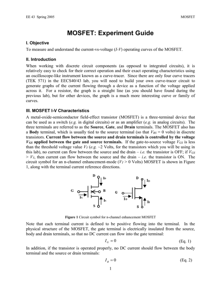
EE 43 Spring 2005 MOSFET MOSFET: Experiment Guide I. Objective To measure and understand the current-vs-voltage (I-V) operating curves of the MOSFET. II. Introduction When working with discrete circuit components (as opposed to integrated circuits), it is relatively easy to check for their correct operation and their exact operating characteristics using an oscilloscope-like instrument known as a curve-tracer. Since there are only four curve tracers (TEK 571) in the EECS40/43 lab, you will need to build your own curve-tracer circuit to generate graphs of the current flowing through a device as a function of the voltage applied across it. For a resistor, the graph is a straight line (as you should have found during the previous lab), but for other devices, the graph is a much more interesting curve or family of curves. III. MOSFET I-V Characteristics A metal-oxide-semiconductor field-effect transistor (MOSFET) is a three-terminal device that can be used as a switch (e.g. in digital circuits) or as an amplifier (e.g. in analog circuits). The three terminals are referred to as the Source, Gate, and Drain terminals. The MOSFET also has a Body terminal, which is usually tied to the source terminal (so that VBS = 0 volts) in discrete transistors. Current flow between the source and drain terminals is controlled by the voltage VGS applied between the gate and source terminals. If the gate-to-source voltage VGS is less than the threshold voltage value VT (e.g. ~2 Volts, for the transistors which you will be using in this lab), no current can flow between the source and the drain – i.e. the transistor is OFF; if VGS > VT, then current can flow between the source and the drain – i.e. the transistor is ON. The circuit symbol for an n-channel enhancement-mode (VT > 0 Volts) MOSFET is shown in Figure 1, along with the terminal current reference directions. D G ID B IG IS S Figure 1 Circuit symbol for n-channel enhancement MOSFET Note that each terminal current is defined to be positive flowing into the terminal. In the physical structure of the MOSFET, the gate terminal is electrically insulated from the source, body and drain terminals, so that no DC current can flow into the gate terminal: IG 0 (Eq. 1) In addition, if the transistor is operated properly, no DC current should flow between the body terminal and the source or drain terminals: IB 0 1 (Eq. 2) EE 43 Spring 2005 MOSFET From Kirchhoff’s Current Law, we know that the sum of all the terminal currents flowing into the MOSFET must be zero: IG I D I B I S 0 (Eq. 3) Substituting Eq. 1 and Eq. 2 into Eq. 3, we obtain I S I D (Eq. 4) Thus, all of the current that flows into the drain terminal flows out of the source terminal. In the ON state, the current IDS flowing from the drain to the source will depend on the potential difference VDS between the drain and the source: IDS increases with increasing drain-to-source voltage VDS as long as the drain voltage is at least VT below the gate voltage, i.e. as long as VGSVT > VDS. When VDS increases above VGS-VT, IDS saturates at a constant value (i.e. it no longer increases with increasing VDS.) Figure 2 shows the I-V operating curves for a typical n-channel enhancement-mode Field Effect Transistor (FET). As can be seen in the figure, for each value of VGS there is a unique curve of IDS vs. VDS. Figure 2 Current IDS flowing through the drain to source of an n-channel MOSFET versus the voltage VDS across drain to source, parameterized by the voltage VGS applied across the gate to source. Figure 3 Curve-tracer circuit 2 EE 43 Spring 2005 MOSFET IV. Hands On 1. Build the curve-tracer circuit. Use RM = 1k. Apply a 10 VPP sine wave at 100 Hz. 2. Invert Channel A1 by pressing the A1 button in the analog section and select Invert On. Put the scope in the XY mode: press the Main/Delayed button, followed by the XY softkey. Use the analog position knobs to put the origin (0V, 0A) of the I-V plot in a convenient location. 3. Insert a resistor as the DUT, and measure the resistance RDUT using the cursors. Keep in mind that the Y-axis is related to the device current: VA2 = I RM. 4. Next, try using an LED as the DUT. Place the cathode (-) at ground. Adjust the analog volts/div until the curve fills the screen as much as possible. 5. Sketch the curve, making sure to indicate the voltage scales on each axis. Note the approximate voltage where the diode “turns on.” 6. Reverse the LED and sketch the curve again. 7. Insert a 0.1 F capacitor as the DUT. Vary the signal frequency to see what happens. Why does the capacitor produce this peculiar curve? Sketch the curve at a frequency and scaling that produces an open ellipse. 8. Next we'll make some changes to the circuit to allow us to measure n-channel MOSFET curves. Remember that a transistor is a three-terminal device, and that an n-channel MOSFET requires a positive voltage across the gate to source to allow a current to flow from the drain to the source. You will provide this voltage with the DC power supply. Figure 4 MOSFET curve tracer 9. Change RM to 51 ohms. Set the 6V power supply to 0V initially, and connect it to the gate and source of the MOSFET as shown in the schematic. Note the pin designations D, G, S. 10. You will need to incrementally raise the voltage on the gate to see the I-V curve change. Use the position knobs to move the origin to the lower left corner of the scope screen. Sketch the family of curves for VGS = 2.5, 2.6, 2.7 ... 3.1V. Be sure to clearly mark each curve with its corresponding VGS. Use the Auto-Store button to store I-V curves on the screen. 3

