PLL & Timing Glossary
February 2002, ver. 1.0
Altera® StratixTM devices have enhanced phase-locked loops (PLLs) that
provide designers with flexible system-level clock management that was
previously only available in discrete PLL devices. Stratix embedded PLLs
meet and exceed the features offered by these high-end discrete devices,
reducing the need for other timing devices in the system. This document
provides a glossary of PLL and timing terminology.
B
Bank skew See Skew, bank.
Board design skew (extrinsic skew)
skew).
See Skew, board design (extrinsic
C
Clock-driver skew (intrinsic skew)
See Skew, clock-driver (intrinsic skew).
Cross-talk induced jitter See Jitter, cross-talk induced.
Cycle-to-cycle jitter See Jitter, cycle-to-cycle.
D
Downstream PLLs See PLLs, downstream.
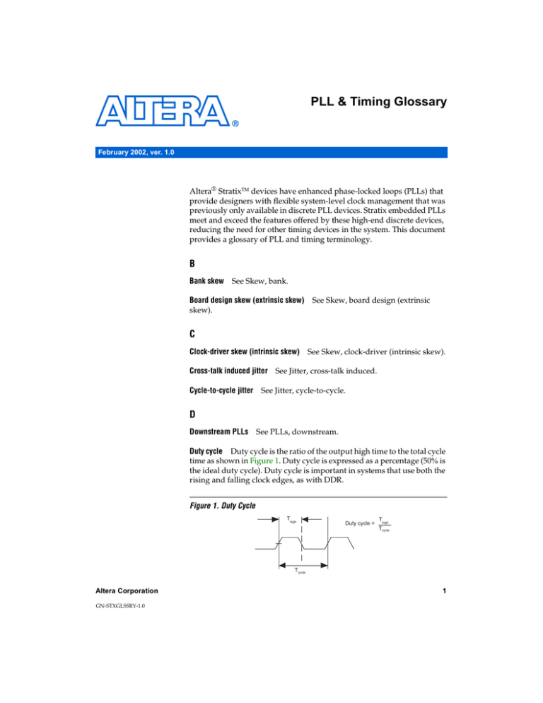
Duty cycle Duty cycle is the ratio of the output high time to the total cycle
time as shown in Figure 1. Duty cycle is expressed as a percentage (50% is
the ideal duty cycle). Duty cycle is important in systems that use both the
rising and falling clock edges, as with DDR.
Figure 1. Duty Cycle
Thigh
Duty cycle =
Thigh
Tcycle
Tcycle
Altera Corporation
GN-STXGLSSRY-1.0
1
PLL & Timing Glossary
E
Extrinsic skew See Skew, board design (extrinsic skew).
H
Half-period jitter See Jitter, half-period.
I
Intrinsic skew
See Skew, clock-driver (intrinsic skew).
J
Jitter Jitter can negatively impact data transmission quality. In many
cases, other signal deviations, like signal skew and coupled noise are
combined and labeled as jitter.
Jitter is the deviation in a clock’s output transitions from its ideal
positions, as shown in Figure 2. Deviation (expressed in ±ps) can occur on
either the leading edge of a signal or the trailing edge of a signal. Jitter may
be induced and coupled onto a clock signal from several different sources
and is not uniform over all frequencies.
Excessive jitter can increase the bit error rate (BER) of a communications
signal by incorrectly transmitting a data bit stream. In digital systems,
jitter can lead to violation of timing margins, causing circuits to behave
improperly. Accurate measurement of jitter is necessary for measuring the
reliability of a system.
Figure 2. Jitter in Clock Signals
Unit
Interval
Edge location
shifted
Reference
Edge
Edge location
shifted
2
Ideal edge
location
Altera Corporation
PLL & Timing Glossary
Common sources of jitter include:
■
■
■
■
■
■
■
■
Internal circuitry of the PLL
Random thermal noise from a crystal
Other resonating devices
Random mechanical noise from crystal vibration
Signal transmitters
Traces and cables
Connectors
Receivers
Beyond these sources, termination dependency, cross talk, reflection,
proximity effects, VCC sag, ground bounce, and electromagnetic
interference (EMI) from nearby devices and equipment can also increase
the amount of jitter in a device.
Reflection and cross-talk frequency-dependent effects may be amplified if
an adjacent signal is synchronous and in phase. Aside from noise caused
by power supplies and ground, changes in circuit impedance are
responsible for most of the jitter in data transmission circuits.
Three types of jitter exist in PLD designs:
■
■
■
Period jitter
Cycle-to-cycle jitter
Half-period jitter
Jitter, cross-talk induced Cross-talk couples and induces jitter from the
magnetic fields generated by nearby signals that produce impedance
changes in components, connectors, and transmission lines.
Jitter, cycle-to-cycle Cycle-to-cycle jitter is the difference in a clock’s
period from one cycle to the next. Cycle-to-cycle jitter is the most difficult
to measure usually requiring a timing interval analyzer.
As shown in Figure 3, J1 and J2 are the measured jitter values. The
maximum values measured over multiple cycles is the maximum cycle-tocycle jitter.
Altera Corporation
3
PLL & Timing Glossary
Figure 3. Cycle-to-Cycle Jitter
t1
t2
t3
Clock
Jitter J1 = t2 -t1
Jitter J2 = t3 -t2
Jitter, half-period Half-period jitter is the measure of maximum change in
a clock’s output transition from its ideal position during one-half period.
Figure 4 illustrates half-period jitter.
Half-period jitter impacts double data rate (DDR) transfer applications. It
is measured as:
tjit(hper) = thalf period – 1/2 fO where fO is the frequency of the input
signal.
Figure 4. Half-Period Jitter
Yx, FBOUT
Yx, FBOUT
thalf period n
t n+1
1
fO
tjit(hper) = thalf period n
1
2*fO
Jitter, period Period jitter is the change in a clock’s output transition,
typically the rising edge, from its ideal position over consecutive clock
edges. Period jitter is measured and expressed in time or frequency.
Period jitter measurements are used to calculate timing margins in
systems, such as tSU and tCO.
As an example, the rising edge of a clock can occur before data is valid on
the data bus on a processor-based system that requires 4 ns of data set-up
time coupled with a clock driving the processor with a maximum of 5 ns
period jitter. The processor may capture incorrect data and the system will
not operate. This is shown in Figure 5.
4
Altera Corporation
PLL & Timing Glossary
Figure 5. Period Jitter Affecting Set-up Time
FIN
FREF
N
FVCO
Up
Charge
Pump
PFD
Down
Post-Dividers
Loop
Filter
& VCO
FOUT1b
K
V
FOUT1a
FOUT2
Feedback
M
Jitter, reflection-induced A major source of jitter is signal reflection caused
by a mismatch in termination impedance. Even when a line is properly
terminated with a value matching the characteristic impedance of the line,
the real part of the impedance changes with frequency. The induced jitter
becomes frequency-dependent.
M
Modulation width Modulation width is the relative variation in the
instantaneous output frequency resulting from spread-spectrum
modulation. The wider the modulation, the larger the band of frequencies
over which the energy is distributed and the more reduction from the
peak. Table 1 lists modulation width.
Table 1. Modulation Width
Type of Spread
Definition
Center spread
The nominal output frequency is specified, and the
spreading results in instantaneous frequencies both
above and below the nominal frequency.
Down spread
The maximum output frequency is specified, and the
spreading results in instantaneous frequencies at or below
the maximum specified.
Example: 100 MHz + 0.5% = 99.5 to 100.5 MHz
Example: 100 MHz _ 0.5% = 99.5 to 100 MHz
Altera Corporation
5
PLL & Timing Glossary
Modulation profile Modulation profile is the waveform of the spreading
signal, which is the low frequency signal that is added to modulate the
output. The band of frequencies over which the EMI energy is spread is
fixed by the modulation width and does not vary with the modulation
profile. Since EMI testing evaluates peaks, spreading energy evenly over
the frequency band lowers EMI. A flat spectral profile with minimal
peaking shows that the energy is evenly spread across the frequency
band.
The following are three types of modulation profiles used in spreadspectrum technology:
■
■
■
Optimized (Lexmark or Hershey’s Kiss) modulation
Linear (Triangular) modulation
Sine wave form modulation
Figure 6 shows the spectrum of these modulation profiles.
Figure 6. Modulation Profiles in Spread Spectrum
Optimized
Modulation
Linear
Modulation
Sine Wave
Modulation
P
Period jitter See Jitter, period.
Phase Locked Loop (PLL) A PLL is a closed-loop frequency-control system
based on the phase difference between the input signal and the output
signal of a controlled oscillator. PLLs can correct large and small
frequency phase discrepancies through rough and fine tuning,
respectively.
As shown in Figure 7, a PLL consists of a pre-divide counter (the N
counter), a phase-detect circuit, a charge pump, a loop filter, a voltage
controlled oscillator (VCO), a feedback counter (M), and post-divide
counters (K or V).
6
Altera Corporation
PLL & Timing Glossary
Figure 7. Block Diagram of a PLL
FIN
FREF
FVCO
Up
N
Charge
Pump
PFD
Down
Post-Dividers
Loop
Filter
& VCO
FOUT1b
K
V
FOUT1a
FOUT2
Feedback
M
The phase detector detects the difference in phase and frequency between
its reference clock and feedback clock inputs and generates “up” or
“down” control signals, based on whether the feedback frequency is
lagging or leading the reference frequency. These two control signals are
then passed through a charge pump and a loop filter to convert the phase
difference to a control voltage, which controls a VCO.
Based on the control voltage, the VCO oscillates at a higher or lower
frequency, which affects the phase and frequency of the feedback clock.
The VCO stabilizes once the reference clock and the feedback clock have
the same phase and frequency.
Inserting the M counter in the feedback path causes the VCO to oscillate
at a frequency that is M times the reference clock frequency. If the output
of the VCO is tapped, a clock frequency of M × FIN is generated, where
FIN is the frequency of the reference clock.
The VCO output frequency is FVCO = FIN × M/N.
The output frequency of the PLL can be expressed as
FOUT = (FIN × M)/(N × K).
The reference frequency of the phase-detect circuit can be expressed as
FREF = FIN /N.
where:
■
■
■
■
■
■
Altera Corporation
FVCO = VCO frequency
FIN = input frequency
FREF = reference frequency
M = multiplier, lies in feedback path
N = divider, lies in reference path
K or V = post divider
7
PLL & Timing Glossary
PLL acquisition/lock time the acquisition/lock time of a PLL is the amount
of time required by the PLL to attain the target frequency after power-up,
or after a programmed output frequency change.
PLLs, downstream A downstream PLL is a device that receives a
reference-timing signal from another PLL-based device, including devices
that use spread-spectrum.
Some examples of downstream PLLs are:
■
■
■
A PLL cell in an ASIC that receives an external reference signal
A PLL-based timing module that generates timing signals by
multiplying an external reference
A zero-delay buffer used on a memory module to buffer the clock
signal
PLL resolution the resolution of a PLL is based on the number of bits in the
M and N counter. The resolution determines the frequency increment
size.
PLL sample rate The sample rate of a PLL determines how often the
inputs are sampled in order to perform phase and frequency correction. It
is expressed as FREF/N.
PLL-to-PLL skew See Skew, PLL-to-PLL.
R
Reflection-induced jitter See Jitter, reflection-induced.
S
Skew Skew is the variation in arrival time of two signals that were
expected to arrive at the same time. Skew is composed of intrinsic skew
and extrinsic skew. Skew can be positive or negative, based on leading or
lagging signals, as shown in Figure 8.
8
Altera Corporation
PLL & Timing Glossary
Figure 8. Skew Caused by Leading & Lagging Signals
Skew
(Lagging)
Output 1
(Reference)
Output 2
Output 3
Skew
(Leading)
In high-speed systems, clock skew greatly affects the timing margin. For
example, skew of 2 ns represents a significant portion of a 10-ns cycle time
for a 100 MHz system. If the timing budget does not allow for this
variation, the system may become unreliable or crash.
Skew, bank Bank skew is the magnitude of the time difference between
the outputs of a single device with a single driving input as shown in
Figure 9.
Figure 9. Bank Skew
V(test)
V ref
0V
V OH
V ref
V OL
INPUT
BANK 1
OUTPUT 1
BANK 1
OUTPUT 2
Altera Corporation
t sk(b)
t sk(b)
9
PLL & Timing Glossary
Skew, board design (extrinsic skew) Extrinsic skew (board design skew) is
caused by layout variation of board traces. Board design skew is the
amount of skew caused by board layout issues. Table 2 lists the factors
associated with board design skew.
Table 2. Board Design Skew Issues
Condition
Definition
Trace Length
The amount of time for a signal to propagate down a trace
depends on the material of the circuit board and the length
of the trace.
Threshold voltage
variation (receiving
device)
If a receiving device has a threshold voltage of 1.2 V, and
another device has a threshold voltage of 1.5 V, and the
rise time of the input signal is
1.0 V/ns, then the two devices will switch 300 ps apart,
causing skew.
Capacitive loading
Differences in capacitive loading on traces cause
differences in the clock rise times at the load. This affects
the time at which the clock edge crosses the input
threshold, causing skew.
Transmission line
termination
With the fast edge rates in clock drivers, traces longer than
4 inches are considered transmission lines. Without
proper termination, these lines exhibit transmission line
effects, like voltage reflections, which cause skew.
Skew, clock-driver (intrinsic skew) Intrinsic skew is the output skew of the
driving device. Intrinsic jitter is caused by the clock driver itself. Most
clock-driver skew is caused by differences in output loading. PLL-based
device skew can be very small, since the device can be adjusted to
compensate for this type of skew.
Skew, PLL-to-PLL PLL-to-PLL skew is the magnitude of the difference in
propagation delay times between any specified terminals of two separate
devices when both devices operate with the same input signals, the same
supply voltages, and the same temperature. Figure 10 illustrates PLL-toPLL skew (tSK(b)).
Figure 10. PLL-to-PLL Skew
V OH
V ref
V OL
OUTPUT 1
t sk(pp)
OUTPUT 2
10
t sk(pp)
V OH
Vref
V OL
Altera Corporation
PLL & Timing Glossary
Spread-spectrum clocking Spectral spreading to modify clock signals
helps minimize radiated emissions. The goal of CPU manufacturers is to
continue to reduce system level EMI.
While circuit designers have traditionally tried to minimize jitter in clock
circuits, a tendency towards intentionally introducing jitter is emerging.
Adding jitter to a system can actually improve EMI/RFI performance.
Spread-spectrum clocking schemes distribute the energy of the
fundamental clock frequency to minimize peaking of energy at specific
frequencies. This reduces the fundamental clock frequency EMI/RFI as
well as the higher frequency harmonic components. Figure 11 shows how
spread-spectrum clocking works.
By reducing the spectrum peak amplitudes, a device will meet stringent
EMI/RFI emission compliance tests and will be more tolerant of EMI/RFI
radiation. Spread-spectrum clocking is less expensive than traditional
EMI/RFI suppression techniques.
Applications for products with the spread-spectrum feature include clock
generators for high-speed RISC or CISC microprocessor systems, such as
embedded microcontroller products, laser printers, and copiers.
Figure 11. Effect of Spread-Spectrum Clocking on EMI Radiation
Amplitude
EMI Reduction
B
A
Frequency
References
■
■
■
■
Altera Corporation
High-Speed Digital Design: A Handbook of Black Magic, Howard Johnson
and Martin Graham, PTR Prentice-Hall. New Jersey, 1993.
Phase Lock Loops: Design, Simulation, and Application 3rd Edition,
McGraw-Hill.
T11.2/Project 1230/Rev. 10 Fiber Channel - Methodologies for Jitter
Specification. Blacklick, Ohio. 1997.
JEDEC Standard 65-A (JESD65-A)
11
PLL & Timing Glossary
101 Innovation Drive
San Jose, CA 95134
(408) 544-7000
http://www.altera.com
Applications Hotline:
(800) 800-EPLD
Literature Services:
lit_req@altera.com
12
Copyright © 2002 Altera Corporation. All rights reserved. Altera, The Programmable Solutions Company, the
stylized Altera logo, specific device designations, and all other words and logos that are identified as
trademarks and/or service marks are, unless noted otherwise, the trademarks and service marks of Altera
Corporation in the U.S. and other countries. All other product or service names are the property of their
respective holders. Altera products are protected under numerous U.S. and foreign patents and pending
applications, maskwork rights, and copyrights. Altera warrants performance of its
semiconductor products to current specifications in accordance with Altera's standard
warranty, but reserves the right to make changes to any products and services at any time
without notice. Altera assumes no responsibility or liability arising out of the application
or use of any information, product, or service described herein except as expressly agreed
to in writing by Altera Corporation. Altera customers are advised to obtain the latest
version of device specifications before relying on any published information and before
placing orders for products or services.
Altera Corporation
