AIRbus Interface
December 2000 ver. 1.00
Functional Specification 9
Features
Fixed width (8-, 16-, or 32-bit) data transfers (dependent on the width
of the data bus)
Read and write access
Four-way handshaking
Arbitrary transaction latency
Single-synchronous operation for higher performance and lower gate
count
Multi-synchronous operation for multiple clock domains
Allows multiple slaves with differing bus widths
The Access to Internal Registers Interface (AIRbus) is a simple and robust
memory-style bus to allow a CPU to read and write registers in various
functional cores within a Complex Programmable Logic Device (CPLD).
In a typical CPLD, the Processor Interface (PIF) block connects to an
external CPU using an industry standard bus such as PCI, PowerPC bus,
68000 bus, 8051 bus. The PIF manages the external bus’s protocol and
converts the latter’s transactions to AIRbus transactions.The PIF is, in
general, the master of the AIRbus.
General
Arrangement
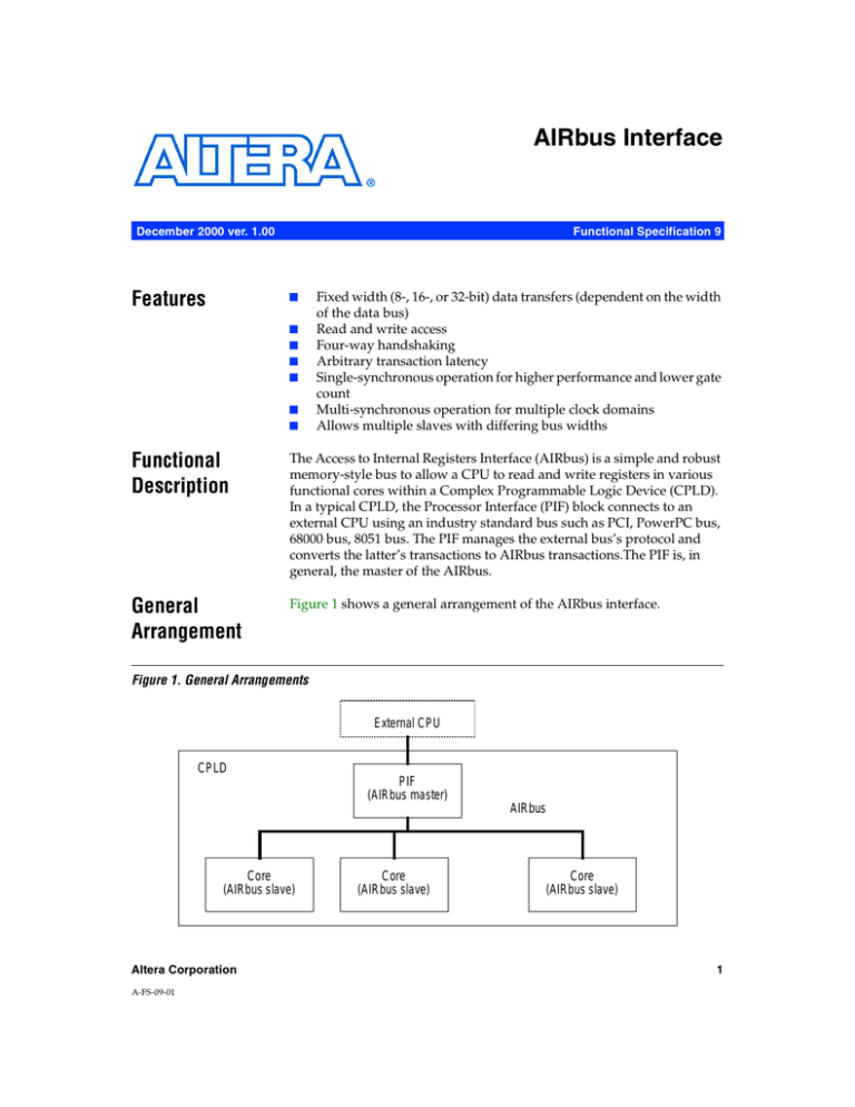
Figure 1 shows a general arrangement of the AIRbus interface.
Figure 1. General Arrangements
External CPU
CPLD
PIF
(AIRbus master)
AIRbus
Core
(AIRbus slave)
Altera Corporation
A-FS-09-01
Core
(AIRbus slave)
Core
(AIRbus slave)
1
13
Development
Tools
Functional
Description
AIRbus Interface Functional Specification
Topology
The AIRbus uses a broadcast topology for signals driven by the master—
typically the PIF. An address decoder, which is separate from the PIF, uses
the most significant bits of the address to demultiplex the sel signal,
producing individual sel outputs for each slave. The least significant bits
of addr, plus wdata and read are broadcast directly to the slaves. Each
slave has its own rdata and dtack output. The module which
instantiates the slaves ORs the dtacks together and feeds the result into
the master’s dtack input. Similarly, it bitwise ORs the rdata of each
slave together. The result is connected to the master’s rdata input.
Figure 2. Example Implementation
External CPU
sel2
sel1
dtack
sel0
Address decode
rdata
low order bits
sel
high order bits
addr
read
wdata
PIF (AIRbus master)
rdata2
Slave 2
dtack2
rdata1
Slave 1
dtack1
rdata0
dtack0
Slave 0
Note:
(1)
2
This OR-busing requires the slaves to set their rdata and dtack outputs to 0 when they are not selected. Each
slave may have an irq output (not shown for clarity). These irqs are ORed together to form the master’s irq input
in the same fashion as dtack.
Altera Corporation
AIRbus Interface Functional Specification
Bus Signals
The clock (clk) is input to all blocks on the AIRbus
In multi-synchronous mode there are multiple clocks
The data bus is either 8, 16 or 32 bits wide. All lines are used on all
cycles. Byte and halfword writes are not possible in the 16- and 32-bit
AIRbuses.
The least significant bit of addr is:
–
0 if rdata and wdata are 8 bits
–
1 if they are 16 bits. addr [0] is considered to be 0 and is not
connected
–
2 if they are 32 bits. addr [1:0] are considered to be 0 and are not
connected
The most significant bit of addr depends on the number of bytes of
address space required. Thus, 8 registers on the 32-bit AIRbus require
32 bytes of address space. addr would then use bits 5:2.
Table 1. Bus Signals
Signal
name
Description
Width
Direction
(master)
Direction
(slave)
Clock
1
Input
Input
sel
Indicates cycle is in progress
1
Output
Input
addr
byte to address of target
application
specific
Output
Input
read
set high during read cycles, low
during write
1
Output
Input
wdata
write data
32/16/8
Output
Input
rdata
data from read
32/16/8
Input
Output
dtack
data transfer acknowledge
1
Input
Output
irq
interrupt request
1
Input
Output
Bus Protocol
13
Development
Tools
clk
Four-Way Handshake
The bus cycles proceed as follows:
Altera Corporation
1.
Master sets wdata (if the cycle is a write), read, and addr
appropriately and asserts sel. The address decoder generates the
appropriate slave select.
2.
Slave observes sel asserted and performs its internal read or write
operation.
3.
Upon completing the read or write, the slave drives rdata if the
cycle is a read, and asserts its dtack.
3
AIRbus Interface Functional Specification
4.
Master observes dtack asserted and records rdata if the cycle is a
read. It then negates (drives low) sel. addr and wdata are now
undefined.
5.
The slave observes sel negated. It sets rdata to 0 and negates
dtack.
6.
The master observes dtack negated and may now start a new bus
cycle.
All signals are sampled, asserted, and negated synchronously to the
master’s and slaves’ clock(s). Note that each step may take multiple clock
cycles, e.g. to complete an internal operation or to meet setup time on data
or address lines. The time required is implementation-dependant.
Figure 3 illustrates AIRbus read and write cycle. The clock is omitted for
clarity.
Figure 3. AIRbus Read & Write Cycle
clk
sel
read
addr
write address
wdata
write data
X
read address
X
X
rdata
0
read data
dtack
1
2
3
4
5
6,1
2
3
4
5
Single-Synchronous Mode
This has the highest performance (4 clock cycles for a fast slave) but
requires the master and all slaves to be on the same clock domain. Figure 3
shows transactions on a single-synchronous bus.
4
Altera Corporation
AIRbus Interface Functional Specification
Multi-Synchronous Mode
This mode incurs a penalty of several clock cycles depending on the
relative frequencies and phases of the master and slaves clocks but allows
the master and the slaves to be on different clock domains. This mode
requires a metastability hardening block (two flip-flops clocked by the
slave’s clock) to transfer the sel signal to the slave, and a metastability
hardening block (two flip-flops clocked by the master’s clock) to transfer
the dtack and irq signals to the master. sel is asserted simultaneously
with wdata/read/addr, and dtack is asserted simultaneously with
rdata. The delay inherent in the metastability hardening process, plus
the four-way handshaking, ensures that addr, read, wdata, and rdata
are stable when they are sampled: no metastability hardening is necessary
on these signals. Note that a bus becomes multi-synchronous mode by
including metastability hardening blocks. Figure 4 shows the structure of
a multi-synchronous bus.
Figure 4. Multi-Synchronous Mode
13
clkm
rdata
addr
read
wdata
sel
Development
Tools
Metastability
hardener
dtackh
PIF (AIRbus master)
dtack
sel1
sel0
Address decode
Metastability
hardener
sel0h
clk0
Altera Corporation
Slave 0
Metastability
hardener
sel1h
clk1
Slave 1
5
AIRbus Interface Functional Specification
Figure 5 illustrates transactions on a multi-synchronous bus (See “Bus
Protocol” on page 3).
Figure 5. Multi-Synchronous Read/Write
clkm
clk0
sel
selh
read
addr
address
X
wdata
write data
X
rdata
0
read data
dtack
dtackh
1
2
3
4
5
6, 1
Internal Width Conversion
In general, the internal AIRbus is as wide as the widest slave. In this case,
all registers are aligned to the natural boundaries of the bus and are
padded in the most significant bits with zeros.
6
On a 32-bit bus:
–
8 bit slaves appear as 32-bit slaves with the data carried on bits
[7:0]. rdata bits [31:8]are set to 0. wdata bits [31:8]are ignored.
Slave addr[0] connects to master addr[2].
–
16 bit slaves appear as 32-bit slaves with the data carried on bits
[15:0]. rdata bits [31:16]are set to 0. wdata bits [31:16]are
ignored. Slave addr[0] connects to master addr[1].
On a 16-bit bus, 8 bit slaves appear as 16-bit slaves with the data
carried on bits [7:0]. rdata bits [15:8]are set to 0. wdata bits [15:8]are
ignored. Slave addr[0] connects to master addr[1].
Altera Corporation
AIRbus Interface Functional Specification
Tables 2 and 3 show how the slave address ports map onto the master’s
address bits.
Table 2. Data Bus Mapping
Slave data bus width (bits)
Master
bus
width
(bits)
8
16
32
slave wdata/rdata [7:0]
connects to:
slave wdata/rdata [15:0]
connects to:
slave wdata/rdata [31:0]
connects to:
8
Master wdata/rdata[7:0]
Illegal
Illegal
16
Master wdata/rdata[7:0]
Master wdata/rdata[15:0]
Illegal
32
Master wdata/rdata[7:0]
Master wdata/rdata[15:0]
Master wdata/rdata[31:0]
Table 3. Address Bus Mapping
Slave data bus width (bits)
8
16
13
32
Master 8
bus
16
width
(bits) 32
Master addr [N-1:0]
Illegal
Illegal
Master addr [N:1]
Master addr [N-1:1]
Illegal
Master addr [N+1:2]
Master addr [N:2]
Master addr [N-1:2]
Unsupported
Bus Operations
Altera Corporation
Dynamic bus sizing or access to partial words
Bus width conversion to external bus
Direct Memory Access (DMA)
Alternate bus masters
Burst transactions
Split transactions
Read-modify-write cycles
7
Development
Tools
slave addr[N-1:0] connects to: slave addr [N-1:1] connects to: slave addr [N-1:2] connects to:
AIRbus Interface Functional Specification
®
101 Innovation Drive
San Jose, CA 95134
(408) 544-7000
http://www.altera.com
Applications Hotline:
(800) 800-EPLD
Customer Marketing:
(408) 544-7104
Literature Services:
lit_req@altera.com
8
Altera, APEX, APEX 20K, MegaCore, MegaWizard, OpenCore, and Quartus are trademarks and/or service
marks of Altera Corporation in the United States and other countries. Altera acknowledges the trademarks of
other organizations for their respective products or services mentioned in this document. Altera products are
protected under numerous U.S. and foreign patents and pending applications, maskwork rights, and
copyrights. Altera warrants performance of its semiconductor products to current specifications in accordance
with Altera’s standard warranty, but reserves the right to make changes to any products and services at any
time without notice. Altera assumes no responsibility or liability arising out of the application or use of any
information, product, or service described herein except as expressly agreed to in writing by Altera
Corporation. Altera customers are advised to obtain the latest version of device
specifications before relying on any published information and before placing orders for
products or services.
Copyright 2000 Altera Corporation. All rights reserved.
Altera Corporation
Printed on Recycled Paper.
