Design Verification Using
the SignalTap II Embedded
Logic Analyzer
January 2003, ver. 1.0
Introduction
Application Note 280
The SignalTap® II embedded logic analyzer, available exclusively in the
Altera® Quartus® II software version 2.2, helps reduce verification times
by allowing you to conduct real-time board level tests of Altera devices.
Traditional methods of verification make it difficult to analyze internal
nodes within an FPGA, because they typically need to be routed to
available I/O pins for data capture with an external logic analyzer. The
SignalTap II analyzer provides access to an FPGA’s internal signals,
allowing you to monitor internal design nodes. This application note
gives an overview of the many new features in the SignalTap II logic
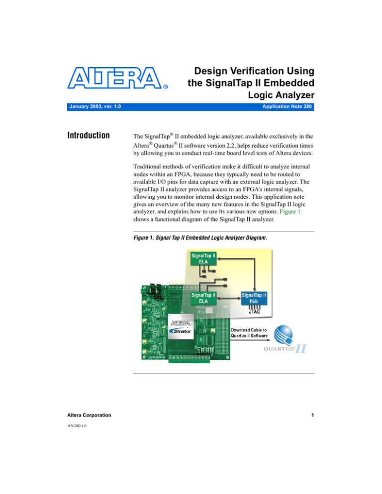
analyzer, and explains how to use its various new options. Figure 1
shows a functional diagram of the SignalTap II analyzer.
Figure 1. Signal Tap II Embedded Logic Analyzer Diagram.
Altera Corporation
AN-280-1.0
1
AN 280: Design Verification Using the SignalTap II Embedded Logic Analyzer
This application note describes how to use the SignalTap II software,
including coverage of the following topics.
■
■
■
■
SignalTap II
Hardware and
Software
Requirements
Hardware and software required when using the SignalTap II logic
analyzer
Configuration options
Using the SignalTap II logic analyzer
Advanced features of the SignalTap II logic analyzer, including
Incremental Routing support
The following hardware and software components are required to use the
SignalTap II logic analyzer:
■
■
The Quartus II software
MasterBlaster™, ByteBlasterMV™, or ByteBlaster II cable
The Quartus II Software
The Quartus II software allows you to select the signals to capture, when
signal capture starts, and how many data samples to capture. You can also
select whether the data is routed to the device’s memory blocks for use by
the SignalTap II logic analyzer, or to the I/O pins for use by external
equipment. Table 1 shows the device support for the SignalTap II logic
analyzer.
Table 1. SignalTap II Device Support
Device
Support
Cyclone™ devices
Full Support in the Quartus II software
version 2.2 service pack 1 (SP1). (1)
Stratix™ GX devices
Full Support in the Quartus II software
version 2.2 service pack 1 (SP1). (1)
Stratix devices
Full Support in the Quartus II software
version 2.1 service pack 1 (SP1). (1)
Excalibur™ devices
Full support
APEX™ II devices
Full support
APEX 20KE devices
Full support
APEX 20KC devices
Full support
APEX 20K devices
Full support
Mercury™ devices
Full support
ACEX™ 1K devices
Not supported
FLEX® 10KE devices
Not supported
FLEX 6000 devices
Not supported
®
MAX 7000B devices
Not supported
Note to Table 1:
(1)
2
Dependent on programming file generation for each device.
Altera Corporation
AN 280: Design Verification Using the SignalTap II Embedded Logic Analyzer
MasterBlaster or ByteBlaster Cable
You can use a MasterBlaster™, ByteBlasterMV™, or ByteBlaster II
communication cable to download configuration data to the device. These
cables are also used to upload captured signal data from the device’s RAM
resources to the Quartus II software. The Quartus II software then
displays data acquired by the SignalTap II logic analyzer as waveforms.
f
SignalTap II
Logic Analyzer
Configuration
Options
See the MasterBlaster Serial/USB Communications Cable Data Sheet, the
ByteBlasterII Parallel Port Download Cable Data Sheet, or the ByteBlasterMV
Parallel Port Download Cable Data Sheet (depending on the cable being
used) for more information.
You can configure the SignalTap II logic analyzer to handle analysis data
by either storing captured data in device RAM or routing captured data to
I/O pins for use by an external logic analyzer or oscilloscope. The
SignalTap II configuration best suited for a design is primarily based on
the following.
■
■
■
the availability of device memory resources and I/O pins
the number of trigger levels being used in analysis
whether or not the SignalTap analyzer is used in conjunction with
external test equipment
Table 2 shows the number of logic elements (LEs) used per number of
signals being analyzed at trigger levels 1, 2, and 3.
Table 2. SignalTap II LE Utilization (1)
Signals
Trigger Level 1
Trigger Level 2
Trigger Level 3
8
219
266
317
16
243
373
466
32
422
596
773
64
689
1033
1383
256
2295
3662
5034
1024
8696
14158
19626
Note to Table 2:
(1)
This table shows LE utilization for a single instance.
1
Altera Corporation
The number of trigger levels employed in analysis increases the
number of LEs required. For an explanation of trigger levels, see
“Specifying Trigger Levels & Trigger Patterns” on page 9.
3
AN 280: Design Verification Using the SignalTap II Embedded Logic Analyzer
Internal RAM Configuration
In the internal RAM configuration, acquired data is saved to the device’s
internal RAM and then streamed off-device via the IEEE Std. 1149.1 Joint
Test Action Group (JTAG) port. This setup requires the most memory
resources, but the fewest number of I/O pins.
The Quartus II software automatically stores acquisition data in the M4K
memory blocks of Cyclone, Stratix, and Stratix GX devices. Table 3 shows
the SignalTap M4K memory block resource usage for these devices per
signal width and sample depth.
Table 3. SignalTap II M4K Block Utilization for Cyclone, Stratix
GX, and Stratix devices (1)
Signals
(Width)
Samples (Width)
256
512
2,048
8,192
8
<1
1
4
16
16
1
2
8
32
32
2
4
16
64
64
4
8
32
128
256
16
32
128
512
Note to Table 3:
(1)
When configuring a SignalTap II analyzer, the Instance Manager reports an
estimate of the memory bits and logic elements required to implement the given
configuration.
The Quartus II software automatically assigns internal memory for
acquisition data storage, which is automatically stored in the embedded
system blocks (ESBs) of APEX II, APEX 20K, APEX 20KE, APEX 20KC,
Mercury, or Excalibur devices. Table 4 shows the SignalTap ESB resource
usage for these devices per signal width and sample depth.
4
Altera Corporation
AN 280: Design Verification Using the SignalTap II Embedded Logic Analyzer
Table 4. SignalTap II ESB Utilization for Cyclone, Stratix GX, and Stratix
devices
Signals
(Width)
Samples (Depth)
128
256
512
1,024
1
2,048
1
2
1
4
8
2
1
2
4
1
2
4
8
16
1
2
4
8
16
32
2
4
8
16
32
64
4
8
16
32
64
128
8
16
32
64
128
Debug Port Configuration
When device RAM is limited, the software can route internal signals to
unused I/O pins for capture by an external analyzer or oscilloscope. This
method is useful for data-intensive applications in which the amount of
saved data exceeds the available sample buffer depth provided by the
device’s RAM.
In the debug port configuration, the Quartus II software automatically
generates pins for signals selected for output via the debug port. To
explicitly assign signals to specific pins, choose Assignments > Assign
Pins.
f
Using the
SignalTap II
Logic Analyzer
Altera Corporation
For more information about the debug port configuration, see “Using the
Debug Port Configuration” on page 12.
Using the SignalTap II logic analyzer involves the following sequence of
steps.
■
■
■
■
■
■
■
Creating a SignalTap II (.stp) file (hereafter referred to as an ‘STP file’)
Assigning signals to the STP file
Assigning an acquisition clock
Specifying the sample depth
Specifying trigger levels and patterns
Compiling the design
Programming the device
5
AN 280: Design Verification Using the SignalTap II Embedded Logic Analyzer
Creating the STP File
The STP file is used to set the logic analyzer settings. Along with the
settings for the analyzer, this file displays the captured data for viewing
and analysis. To create a new STP file, follow these steps.
1.
If you have not already done so, perform an analysis and synthesis,
an analysis and elaboration, or a compilation of the design.
2.
In the Quartus II software, choose File > New.
3.
In the dialog box that appears, click on the Other Files tab and select
SignalTap II file.
4.
Click OK.
Figure 2 shows an example of a new STP file.
Figure 2. SignalTap II File
Assigning Signals to the STP File
To assign signals to the STP file, perform the following steps.
1.
6
In the SignalTap II Logic Analyzer window, click the Setup tab.
Altera Corporation
AN 280: Design Verification Using the SignalTap II Embedded Logic Analyzer
2.
Double-click on the Node Name column, which is above the Setup
tab.
3.
Set the Node Finder filter to either SignalTap II Pre-Synthesis, or
SignalTap II Post-Fitting.
Setting the filter to SignalTap II Pre-Synthesis in the nodefinder will
find signals within the design that have been preserved prior to
Quartus II performing synthesis. Setting the filter to SignalTap II
Post Fitting in the nodefinder will find signals within the design that
have been preserved after Quartus II has fitted the design in the
target device family. The Incremental Route feature will
automatically be used with any node found with the be used with
the SignalTap II Post Fitting filter.
f
For more information on this feature, go to “Incremental Routing”
on page 14.
To increase the number of signals found with the SignalTap II filters,
disable the Preserve Fewer Node Names to save disk space. This
option can be found under the Mode section of the Compiler
Settings.
4.
In the Named box, enter a node name, partial node name, or
wildcard characters. To start the node name search, click Start.
5.
In the Nodes Found list, select the node or bus you want to add to
the STP file.
6.
To copy the selected node names to the Selected Nodes list, click “>”
or “>>.”
7.
To insert the selected nodes in the STP file, click OK.
Assigning An Acquisition Clock
The acquisition clock is used for data sampling, which occurs on every
rising edge of the acquisition clock. The speed at which you can run the
sample clock varies from one design to the next. The Quartus II static
timing analyzer displays the maximum acquisition clock frequency.
1
Altera Corporation
For best results, assign a global clock to be the SignalTap II
acquisition clock signal.
7
AN 280: Design Verification Using the SignalTap II Embedded Logic Analyzer
If you do not assign the clock signal in the SignalTap II window, the
Quartus II software automatically creates a clock pin called
auto_stp_external_clk. You must then make an explicit pin
assignment for auto_stp_external_clk and connect this pin to an
external signal. This signal acts as the acquisition clock for the analyzer.
To assign an acquisition clock, perform the following steps.
1.
In the SignalTap II Logic Analyzer window, click the Setup tab.
2.
Click Browse... next to the Clock list to open the Node Finder.
3.
Set the Node Finder filter to either SignalTap II Pre-Synthesis or
SignalTap II Post-Fitting.
4.
In the Named box, enter the name of the signal that you would like
to use as your sample clock.
5.
To start the node search, click Start.
6.
In the Nodes Found list, select the node representing the design’s
global clock signal.
7.
To copy the selected node name to the Selected Nodes list, click ‘>’
or ‘>>.’
8.
Click OK.
The node is now specified as the clock in the SignalTap II window.
Specifying the Sample Depth
The sample depth is the number of samples that are stored for each signal.
When the SignalTap II logic analyzer is configured to use device memory,
use of device memory resources increases in direct relation to the sample
depth.
To set the sample depth, use the Sample Depth pull-down menu in the
Data section of the Setup Tab of the STP file. The sample depth can range
between 0 (zero) and 128K samples. A sample depth of 128K samples
allows you to store and display a large amount of data centered around
the trigger event. A sample depth of zero samples allows you to preserve
memory resources if you only intend to use the debug and/or trigger
in/out ports in the SignalTap II logic analyzer.
8
Altera Corporation
AN 280: Design Verification Using the SignalTap II Embedded Logic Analyzer
Specifying Trigger Levels & Trigger Patterns
You can configure the SignalTap II tool with up to ten trigger levels. This
capability offers a great deal of flexibility and allows you to set complex
triggering conditions, making it easier to isolate the conditions that cause
a functional failure. Multi-level triggering also allows you to view only the
most relevant signal data, thus reducing the number of samples and
making it easier to locate the source of the problem. The multiple trigger
levels are logically ‘ANDED’ together, and, after all of the trigger
conditions are satisfied, data capture will commence.
To specify triggers and triggering levels, perform the following steps.
1.
In the SignalTap II window, click the Setup tab.
2.
In the Trigger Levels list, select the number of trigger levels that you
want to create.
3.
If necessary, in the Trigger column, turn on the trigger option for
each signal that you want to trigger.
4.
Assign a logic condition to each signal that you want to use in the
trigger level, as follows. In the L# (L1 ... L10) column, right-click the
appropriate cell and choose one of the following commands from the
resulting pop-up menu.
–
–
–
–
–
–
Don't Care
Low
Falling Edge
Rising Edge
High
Either Edge
Specifying the Trigger Position
The trigger position setting allows you to specify the amount of data that
is acquired before the trigger event and the amount that is acquired after
the trigger event.
The ratio of pre-trigger data to post-trigger data is adjusted by applying
the following settings.
■
■
■
Altera Corporation
Pre - save signal activity that occurred after the trigger (12% pretrigger, 88% post-trigger).
Center - save half pre-trigger and half post-trigger data.
Post - save signal activity that occurred before the trigger (88% pretrigger, 12% post-trigger).
9
AN 280: Design Verification Using the SignalTap II Embedded Logic Analyzer
■
Continuous - save signal activity indefinitely (until stopped
manually).
Specifying Nodes Allocated for Triggering & Data
This feature allows you to specify the number of signals that can be
analyzed by the SignalTap II logic analyzer. Setting the Nodes Allocated
option to Auto means that Quartus II will build a SignalTap II analyzer to
accomodate the number of data and trigger channels that were selected in
the Setup window. Setting the Nodes Allocated option to Manual allows
you to allocate extra nodes, which can be incrementally routed to postfitting nodes later, without performing a full design compilation. This
feature can significantly reduce compile times when adding or changing
signal selections.
f
See the “Incremental Routing” section on page 14 for more information on
this feature.
To specify whether a node is allocated for triggering, data, or both, scroll
across the row for the node in the SignalTap II window and click on one,
or both, of the checkboxes for Trigger and Data.
Compiling the STP File
The STP file must be compiled with the project to function correctly. You
must recompile the design whenever one the following changes is made
to the STP file.
■
■
■
■
■
■
■
■
adding or removing instances
changing the number of trigger levels
changing the number of signals
assigning signals
changing the sample depth
enabling trigger input or output
changing the trigger input or trigger output source
enabling the debug port
To compile the STP file with your Quartus II project:
10
1.
Choose Assignments > Setting.
2.
In the Category list, select SignalTap II Logic Analyzer under
Compiler Settings.
3.
Click Enable SignalTap II Logic Analyzer.
4.
In the SignalTap II File name box, type the name of the STP file you
want to compile, or select a file name with Browse (...).
Altera Corporation
AN 280: Design Verification Using the SignalTap II Embedded Logic Analyzer
5.
f
Click OK, then recompile the design.
See the “Incremental Routing” section on page 14 for more information on
reducing the time needed to compile an STP file after signals are added or
changed.
Programming the Device for SignalTap II Analysis
To program a device for use with the SignalTap II logic analyzer, follow
these steps.
1.
Under File > JTAG Chain Configuration, select an SRAM Object
File (.sof).
2.
In the Device list, select the device to which you want to download
the design.
1
3.
Advanced
Features
Altera Corporation
If you modify the devices on the circuit board and want to scan
the new devices, perform the following three steps.
a.
Click Scan Chain.
b.
In the Device list, select the device to which you want to
download the design.
c.
Click Program Device.
Run the SignalTap II logic analyzer by selecting Run or AutoRun
from the SignalTap II window.
This section describes the following advanced features:
■
■
■
■
■
■
■
■
■
Multiple Analyzer Instances
Using the Debug Port Configuration
Trigger Input & Trigger Output Configuration
Incremental Routing
Data Log
Instance Manager
Waveform Export Utility
Mnemonic Table
SignalTap II Health Monitor
11
AN 280: Design Verification Using the SignalTap II Embedded Logic Analyzer
Multiple Analyzer Instances
The SignalTap II logic analyzer includes support for multiple embedded
logic analyzers within an FPGA device. This feature allows you to create
a unique embedded logic analyzer for each clock domain that is present in
the design. As multiple unique instances are added to the STP file, the LE
count increases proportionally.
In addition to debugging multiple clock domains, this feature allows you
to apply the same SignalTap II settings to a group of signals within the
same clock domain. For example, if you have a set of signals that need to
use a sample depth of 64K, while another set of signals within the same
clock domain need a 1K sample depth, you can create two unique
instances to meet these needs.
To create multiple analyzers, select Edit > Create Instance, or right-click
in the Instance Manager window, and select Create Instance.
Using the Debug Port Configuration
When device RAM is limited, the software can route internal signals to
unused I/O pins for capture by an external analyzer or oscilloscope. The
debug port configuration conserves memory at the expense of I/O pins. It
is useful for data-intensive applications in which the amount of saved
data exceeds the available sample buffer depth provided by the device’s
RAM.
In the debug port configuration, the Quartus II software automatically
generates pins for signals selected for output via the debug port. To use
the SignalTap II Analyzer debug port configuration, follow these steps.
1.
Click a signal in the Out column.
2.
Choose Edit > Enable Debug Port.
3.
If you want to rename the debug port pin, type the new name in the
Out column.
The default signal name for the debug ports is
auto_stp_debug_out_<m>_<n>, where m refers to the instance
number and n refers to the signal number.
4.
12
Manually assign the debug port signal name to an unused I/O pin.
Altera Corporation
AN 280: Design Verification Using the SignalTap II Embedded Logic Analyzer
Trigger Input & Trigger Output Configuration
The SignalTap II logic analyzer can use a trigger input for triggering by an
external source. The analyzer can also be operated in the trigger output
configuration in which it supplies an external signal to trigger other
devices. Using these features allows you to synchronize the internal
embedded logic analyzer to external logic analysis equipment.
Using Trigger In
To use Trigger In, perform the following steps.
1.
In the SignalTap II logic analyzer, click the Setup tab.
2.
In the Signal Configuration window pane, click the Trigger In
checkbox.
3.
In the Pattern pulldown list, select the condition you would like to
act as your trigger event.
4.
Click on the Browse button (...), next to the Trigger In, Source field.
When the Node Finder window appears, select an input pin in your
design by setting the Trigger In source.
Using Trigger Out
To use Trigger Out, perfom the following steps:
1.
In the SignalTap II window, click the Setup tab.
2.
In the Signal Configuration window pane, click the Trigger Out
checkbox.
3.
In the Level list, select the condition you would like to signify the
trigger event is occurring.
4.
Click on the Browse button (...), next to the Trigger out, Target field.
When the Node Finder window appears, select an output pin in
your design by setting the Target.
Using Trigger Out of One Analyzer as the Trigger In of Another Analyzer
An advanced feature of the SignalTap II Logic Analyzer is the ability to
enable the Trigger Out of one analyzer and use this signal as the Trigger
In to another analyzer. This feature allows you to synchronize and debug
events that occur across multiple clock domains.
Altera Corporation
13
AN 280: Design Verification Using the SignalTap II Embedded Logic Analyzer
Incremental Routing
The incremental routing feature allows you to analyze internal device
nodes without affecting the existing placement and routing in a design.
SignalTap II incremental routing shortens the debug process by allowing
you to analyze post-compilation nodes without performing a full
recompile.
Before using the SignalTap II incremental routing feature, you must
perform the following three steps.
■
■
■
Set the number of nodes allocated
Select any nodes reserved for incremental routing
Perform a Smart Compilation
Set the Number of Nodes Allocated
Set the Nodes Allocated button to Manual, as shown in Figure 3, and
enter a value that includes the number of nodes you want to analyze, plus
any extra nodes you may want to incrementally add later in the
verification process.
f
See “Specifying Nodes Allocated for Triggering & Data” on page 10 for
more details on this subject.
Figure 3. Nodes Allocated
Select Nodes Reserved for Incremental Routing
As shown in Figure 4, the Signal Tap II Setup window shows presynthesis nodes and post-fitting nodes, and a column with Incremental
Route (shown as Inc Rte) checkboxes. Post-fitting nodes are displayed in
blue, with the Inc Rte checkbox enabled and grayed out, so that it cannot
be edited.
14
Altera Corporation
AN 280: Design Verification Using the SignalTap II Embedded Logic Analyzer
By enabling the Inc Rte checkbox on pre-synthesis nodes, you will
preserve the signal to the fitting stage of the compilation. You can later
delete the incrementally-routed pre-synthesis node and replace it with a
post-fitting node. The post-fitting node will be incrementally routed to
reduce compilation time, and will not increase the number of nodes
needed to implement the SignalTap II analyzer.
Figure 4. The SignalTap II Setup Window (1)
Note to Figure 4:
(1)
Post-fitting nodes are dislayed in blue, and Inc Rte is always checked for postfitting.
Perform a Smart Compilation
Before using the SignalTap II incremental routing feature, you must
perform a “smart” compilation. This is accomplished by enabling the
Automatically turn on smart compilation if conditions exist in which
SignalTap II with incremental routing is used option. This option is
available from the SignalTap II logic analyzer page of the Assignment
Settings dialog box.
Altera Corporation
15
AN 280: Design Verification Using the SignalTap II Embedded Logic Analyzer
After the design is compiled with Smart Compilation enabled, you will be
able to add additional nodes to the analyzer (provided sufficient nodes are
allocated), or delete a pre-synthesis node with the Inc Rte box checked,
and replace it with a post-fitting node. You can also delete a post-fitting
node and replace it with another post-fitting node, without performing a
full design recompile. The Smart Recompile feature will perform a quick
incremental routing compilation to add the additional nodes to your
SignalTap II logic analyzer, under the following conditions.
■
■
you do not add more nodes than were allocated in the previous
compilation
you did not delete a pre-synthesis node without the Inc Rte checkbox
enabled
Data Log
The data log shows a history of captured data that is acquired with the
SignalTap II logic analyzer. The analyzer acquires data and then stores it
in a log and displays it as a waveform. The default name for the log is a
timestamp based on when the data was acquired. The logs are organized
in a hierarchical manner; similar logs of captured data are grouped
together in Trigger Sets. To recall a data log from a given trigger set,
double click on the data log.
Instance Manager
This feature, which is important when FPGA resources are limited, allows
you to determine SignalTap II resource usage before the compilation. You
can tailor the SignalTap II settings based on the available resources. As the
SignalTap II configuration is modified, the Instance Manager values are
dynamically updated to show estimated LE and memory usage. Figure 5
shows the estimated LE and memory usage for two instances.
Figure 5. The Instance Manager Window
16
Altera Corporation
AN 280: Design Verification Using the SignalTap II Embedded Logic Analyzer
Waveform Export Utility
This feature allows you to export the acquired data to industry-standard
formats that can be used with third-party simulation tools. The export file
types are:
■
■
■
■
Comma Separated Values (.csv)
Table File (.tbl)
Value Change Dump (.vcd)
Vector Waveform File (.vwf)
To export SignalTap II captured data, choose Export.
Mnemonic Table
You can configure the SignalTap II Logic Analyzer to create mnemonic
tables for a group of signals. The mnemonic table feature allows a set of
bit patterns to be assigned to a predefined name, making captured data
more meaningful. To create a mnemonic table, right-click in the Setup
view of an STP file and select Mnemonic Setup. To assign a group of
signals to a mnemonic value, right-click on the group, and select Bus
Display Setup.
SignalTap II Health Monitor
This feature provides you with useful information on the status of the
SignalTap II logic analyzer. Click the Help icon next to the message to
obtain additional details about the message.
Conclusion
Altera Corporation
As the device geometry of FPGAs decrease in size, verification engineers
will find it increasingly difficult to access device I/O pins for debugging
purposes. With the aid of the SignalTap II logic analyzer, this problem
becomes virtually non-existent.
17
AN 280: Design Verification Using the SignalTap II Embedded Logic Analyzer
101 Innovation Drive
San Jose, CA 95134
(408) 544-7000
http://www.altera.com
Applications Hotline:
(800) 800-EPLD
Literature Services:
lit_req@altera.com
18
Copyright © 2003 Altera Corporation. All rights reserved. Altera, The Programmable Solutions Company, the
stylized Altera logo, specific device designations, and all other words and logos that are identified as
trademarks and/or service marks are, unless noted otherwise, the trademarks and service marks of Altera
Corporation in the U.S. and other countries. All other product or service names are the property of their
respective holders. Altera products are protected under numerous U.S. and foreign patents and pending
applications, maskwork rights, and copyrights. Altera warrants performance of its
semiconductor products to current specifications in accordance with Altera's standard
warranty, but reserves the right to make changes to any products and services at any time
without notice. Altera assumes no responsibility or liability arising out of the application
or use of any information, product, or service described herein except as expressly agreed
to in writing by Altera Corporation. Altera customers are advised to obtain the latest
version of device specifications before relying on any published information and before
placing orders for products or services.
Altera Corporation
