vii iii iv
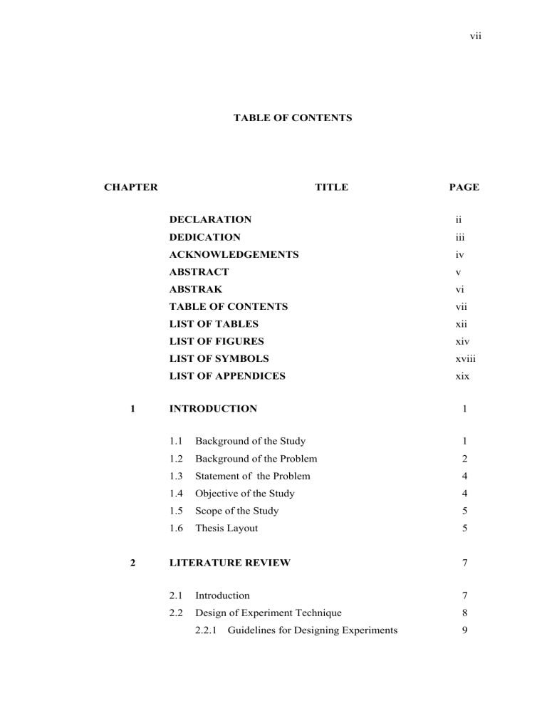
TABLE OF CONTENTS
CHAPTER
DECLARATION
DEDICATION
ACKNOWLEDGEMENTS
ABSTRACT
ABSTRAK
TABLE OF CONTENTS
LIST OF TABLES
LIST OF FIGURES
LIST OF SYMBOLS
LIST OF APPENDICES
TITLE
1 INTRODUCTION
1.1
Background of the Study
1.2
Background of the Problem
1.3
Statement of the Problem
1.4
Objective of the Study
1.5
Scope of the Study
1.6
Thesis Layout
2 LITERATURE REVIEW
2.1 Introduction
2.2 Design of Experiment Technique
2.2.1
Guidelines for Designing Experiments vii
PAGE vi vii xii xiv ii iii iv v xviii xix
1
4
4
1
2
5
5
7
7
8
9
viii
2.3
Electroplating Technique
2.3.1
Electrochemical Terms
2.3.2
Electroplating Equipment for Nickel and
Chromium Electroplating
2.3.3
Electroplating Process
2.3.4
Nickel Electroplating
2.3.4.1
Properties of Nickel
2.3.4.2
The Reason of Using Nickel prior
Chromium
2.3.4.3
The Basic of Nickel Electroplating
Process
2.3.4.4
Hydrogen Evolution and Cathode
9
10
11
14
15
15
15
16
2.3.4.5
Efficiency
Anode Efficiency
2.3.4.6
Controlling the Solution Composition
2.3.4.7
Controlling pH, Temperature Current
2.3.4.8
Density and Water Quality
Controlling Impurities
2.3.4.9
Nickel Plating Solution Composition
2.3.4.10
Description of Nickel Plating Solution
2.3.5
Compositions
Chromium Electroplating
2.3.5.1
Cathode Efficiency of Chromium Plating
Solutions
19
21
2.3.5.2
Chromium Plating Solution Composition 23
2.4
Historical Background of Diamond Coating 24
2.5
CVD Process
2.5.1
Advantages of CVD Process
26
27
28 2.5.2
Disadvantages of CVD Process
2.5.3
Five Major Characteristics of CVD Diamond
Coating 29
2.5.4
Hot Filament CVD Technique
2.5.4.1
Advantages of HFCVD
2.5.4.2
Disadvantages of HFCVD
22
31
34
34
17
17
17
18
18
18
3 ix
2.5.5
Substrate Material
2.5.5.1
Characteristic of Tungsten Carbide
(WC-Co)
2.5.5.2
Thermal Expansion Coefficient of
Substrate
2.5.6
The Effect of Major Parameters on HFCVD
34
34
36
Diamond Coating on WC-Co
2.5.6.1
The Effect of Methane Concentration
2.5.6.2
The Effect of Reactor Pressure
2.5.6.3
The Effect of Substrate Temperature
37
37
38
38
2.5.6.4
The Effect of Co Binder
2.6
Pre-Treatment Methods in Order to Suppress the Negative
39
Effects of Cobalt
2.6.1
2.6.2
Heat Treatments
Etching of Cobalt Binder
41
42
42
2.6.3
Micro-Roughening of WC-Co Surface Morphology 43
2.6.4
Forming Stable Cobalt Compounds
2.6.5
Giving a Suitable Diffusion Barrier Layer
44
(Interlayer) on the Substrates
2.6.5.1
Critical Review of Suitable Diffusion
45
Barrier Layer on the WC-Co Substrate 45
RESEARCH METHODOLOGY
3.1 Introduction
3.2
Preparing the Substrate Material
3.2.1
Cutting Workpieces by Means of the Linear
Precision Saw (Precision Cutter Machine)
3.3
3.2.2
Measuring the Surface Roughness
3.2.3
Measuring the Weight of Substrate
Pre-Treatment of Substrates
3.4
Electroplating Technique
3.4.1
Electroplating Equipments
3.4.1.1
Tank
54
54
55
62
63
63
56
58
59
59
4 x
3.4.1.2
Heater
3.4.1.3
Rectifier
3.4.1.4
Filter Pump
3.4.2
Nickel Electroplating
3.4.2.1
Nickel Plating Compositions
3.4.2.2
The Nickel Solution
3.4.2.3
Application of Current During Loading
3.4.3
Chromium Electroplating
3.4.3.1
Chromium Plating Compositions
3.4.3.2
Preparation of the Chromium Solution
3.4.3.3
Characteristic of Anode Material in
Chromium Plating
3.4.4
Design of Experiment Technique
3.5
Mounting and Grinding the Substrate
3.6
Characterisation Technique (SEM)
RESULTS AND DISCUSSIONS
4.1 Introduction
4.2 Section One- Part One for Nickel Electroplating
4.2.1
Mathematical and Statistical Analysis
4.2.2
Response - Thickness of Deposition
4.2.2.1
ANOVA Analysis
4.2.2.2
Model Adequacy Checking
4.2.2.3
Normal Probability Plot
4.2.2.4
Main Effect and Interaction Analysis
4.3
Section One – Part Two for Nickel Electroplating
4.3.1
ANOVA Analysis for Deposited Thickness
Response
4.3.2
ANOVA Analysis for Adhesion-Test Time
Response
4.3.3
Results from Both ANOVA Analyses
4.4
Section One – Part Three for Nickel Electroplating
68
69
74
75
76
88
89
91
91
66
66
67
67
63
64
64
65
67
68
78
81
82
83
86
76
76
77
77
xi
4.4.1
Design Expert Output for Thickness of Coating
Response
4.4.1.1
ANOVA Analysis
4.4.1.2
Normal Probability Plot
4.4.1.3
Plot of Residuals versus Fitted Values
4.4.1.4
Surface and Contour Plots
4.4.2
Design Expert Output for Adhesion-Test Time
93
93
96
97
98
Response
4.4.2.1
ANOVA Analysis
99
99
4.4.2.2
Normal Probability Plot 103
4.4.2.3
Plot of Residuals versus Fitted Values 104
4.4.2.4
3D Surface and Contour Plot
4.4.3
Overlay the Contour Plots
4.4.4
Optimum Parameters Combination
4.4.5
Discussion
4.5
Section Two – Chromium Electroplating on
105
106
107
107
108 Nickel Coated Substrate
4.5.1
Design of Experiment for Chromium
Electroplating – Part 1
4.5.1.1
Discussion
4.5.2
Design of Experiment for Chromium
Electroplating – Part 2
4.5.3
Conclusion of Part 1 and Part 2
109
110
112
5 for Chromium Electroplating
CONCLUSIONS AND RECOMMENDATIONS
114
4.6
Final Results of Nickel and Nickel-Chromium Coating 114
4.6.1
SEM Results 115
122
5.1
5.2
Results and Conclusions
Recommendations
REFERENCES
Appendix A
122
125
126
132-134
xii
4.5
4.6
4.7
4.8
4.9
LIST OF TABLES
3.2
3.3
3.4
3.5
4.1
4.2
4.3
2.4
2.5
2.6
3.1
2.1
2.2
2.3
4.4
TABLE NO.
The ANOVA table for response thickness, R1
Factor and level interest for second part of nickel electroplating
Data for part two of nickel electroplating, (the second first-order model)
TITLE
Guidelines for designing an experiment
Materials and their suitable and unsuitable environments
Recommendations of nickel plating solution compositions
Recommendations of chromium plating solution compositions
Some of the outstanding properties of diamond
Typical conditions for diamond deposition in HFCVD
Compositions of nickel plating solution
Compositions of chromium plating solution
The initial factors and levels of interest for nickel electroplating
The second factors and levels of interest for nickel electroplating
Factors and levels of interest for chromium electroplating
Data for part one of nickel electroplating, the first-order model
ANOVA table for response thickness of deposition, R1
ANOVA table for adhesion-test time response, R2
Central composite design for part three of nickel electroplating
Computer output from design-expert for fitting a model to the deposited thickness response in third section of nickel electroplating experiment
Computer output from design-expert for fitting a model to the adhesion-test time response in third section of nickel electroplating experiment
PAGE
87
88
90
92
93
100
70
70
70
78
79
86
25
31
66
68
9
12
19
23
4.10
The optimum parameters combinations for thickness of coating and adhesion-test time responses for nickel electroplating on
WC-Co substrates
4.11
Factor and level interest for chromium electroplating
4.12
Initial data for chromium electroplating on nickel coated substrates
4.13
Plating time in minutes for chromium deposit of average thickness 1-3 micron for current density 12Amp/dm
2
according to the Canning Handbook
4.14
Final results for chromium electroplating on nickel coated substrates xiii
107
109
109
112
113
xiv
LIST OF FIGURES
2.1
2.2
2.3
FIGURE NO. TITLE
Schematic of nickel electroplating on tungsten carbide
Variation in cathode efficiency with current density
Schematic diagram of diamond nucleation and growth in CVD
2.4
2.5
2.6
process
Schematic of a hot filament assisted CVD diamond growth system
Schematic of the physical and chemical process occuring during diamond CVD
Conventional removing of Co from near surface regions of cemented carbides prior to deposition of diamond (left) and proposed method of Co deactivation (right)
2.7
2.8
2.9
Flank wear of diamond coated cutting tools after different pretreatment and coating procedures
Three-dimension profilometry images of wear tracks on WC-
Co, Cr-N-coated, and multilayer (Cr-N+ diamond) coated samples after 30 min dry sliding tests
Wear resistance of diamond coatings on boronized and aluminized insert tips in comparison to conventionally etched samples
2.10
Schematics of the phase transformation in the WCGC during the process of diamond deposition
2.11
Schematic of the surface engineering approach for fabrication of the nano-microcrystalline diamond film composite coating hard metal cutting tools
PAGE
16
22
30
32
33
44
47
48
49
51
53
2.12
Comparison of cutting performance for the microcrystalline and
Nano-micro composite diamond coated WC – 6 wt. % Co
3.1
3.2
3.3
3.4
3.5
inserts subjected to the surface
The outline of project
Row material of WC-Co (before cutting)
Sample of substrate (12×2 mm) (after cutting)
SOMET 4000 linear precision saw
Formtracer CS - 5000 (Roughness/Contour Measuring System) -
Mitutoyo
3.6
3.7
Balance - resolution-10 nanogram
BWT chamber for blasting
3.8
3.9
Harnisch + Rieth D-S 100A steam cleaner
Branson 2510 ultrasonic bath machine
3.10
The nickel and chromium electroplating equipments
3.11
Buehler automatic mounting machine
3.12
Scanning Electron Microscope (SEM) – Philips XL40
4.1
Normal probability plot of residuals 82
4.2
Half-normal probability plot of the effects for the response, R
4.3
The main effects plots for the thickness of coating response, R
4.4
The interaction plot for the thickness of coating response
4.5
Central composite designs for three factors
4.6
Normal probability plot of residuals for thickness of coating response, R1
4.7
The residuals versus the fitted values for the thickness of coating, R1
4.8
The contour plot for the thickness of coating response, R1
4.9
The three-dimensional response surface plot for the Thickness of coating response, R1
4.10
Normal probability plot of residuals for adhesion-test time response, R2
4.11
The residuals versus the fitted values for the adhesion-test time response, R2
4.12
Contour plot of adhesion-test time response, R2 xv
62
65
75
75
58
59
60
61
53
55
56
56
57
83
85
85
92
97
97
98
99
104
104
105
4.13
Three dimensional response surface plots for the adhesion-test time response, R2
4.14
Region of the optimum found by overlaying thickness of coating and adhesion-test time response surface for nickel electroplating on tungsten carbide substrate
4.15
Partial coating of chromium on nickel coated sample at current density 10Amp/dm
2
4.16
Tearing the nickel surface in high current density (20Amp/dm
2
) of chromium electroplating, (a) bath temperature = 40 ºC, (b) and (c) bath temperature = 50 ºC
4.17
Coating the chromium on all surfaces with a slight burning on the surface 15Amp/dm
2
4.18
Slight dull grey rough deposition of chromium in current density
= 12Amp/dm
2
, (a) bath temperature = 36 ºC and (b) bath temperature = 38 ºC
4.19
Bright deposition of chromium on all surfaces in current density
= 12Amp/dm
2
, (a) bath temperature = 40 ºC and (b) bath temperature = 42 ºC
4.20
Nickel coating on WC-Co substrate
4.21
Nickel and nickel-chromium coating on WC-Co substrate
4.22
The mounted cross-sectioned samples
4.23
SEM showing the cross-section and interface morphology and the thickness of nickel coated WC-Co when bath temperature =
70 ºC, current density = 24Amp/dm
2
, and plating time = 40 minutes
4.24
SEM showing the cross-section and interface morphology and the thickness of nickel coated WC-Co when bath temperature =
70 ºC, current density = 8Amp/dm
2
, and plating time = 60 minutes
4.25
SEM showing the cross-section and interface morphology and the thickness of nickel coated WC-Co when bath temperature =
60 ºC, current density = 6Amp/dm
2
, and plating time = 73.6 minutes xvi
105
106
110
111
111
113
114
114
115
116
117
117
118
4.26
SEM showing the cross-section and interface morphology and the thickness of nickel coated WC-Co when bath temperature =
60 ºC, current density = 6Amp/dm
2
, and plating time = 40 minutes
4.27
SEM showing the cross-section and interface morphology and the thickness of nickel coated WC-Co when bath temperature =
50 ºC, current density = 4Amp/dm
2
, and plating time = 60 minutes
4.28
SEM showing the cross-section and interface morphology and the thickness of nickel-chromium coated WC-Co when (for nickel; bath temperature = 58 ºC, current density = 4Amp/dm
2
, and plating time = 26.3 minutes) and (for chromium; bath temperature = 42 ºC, current density = 12Amp/dm
2
, and plating time = 15 minutes)
4.29
SEM showing the cross-section and interface morphology and the thickness of nickel-chromium coated WC-Co when (for nickel; bath temperature = 58 ºC, current density = 4Amp/dm
2
, and plating time = 26.3 minutes, thickness = 6.3µm) and (for chromium; bath temperature = 42 ºC, current density =
12Amp/dm
2
, and plating time = 15 minutes, thickness = 2.44
µm)
4.30
EDX analysis for nickel coating
4.31
EDX analysis for nickel-chromium coating xvii
118
119
119
120
120
121
xviii
LIST OF SYMBOLS
A - First factor or input variable investigated – bath temperature
(ºC)
Adeq. precision - Adequate precision
Adj. R
2
- Adjusted R-square
B - Second factor or input variable investigated – current density
(Amp/dm
2
)
C - Third factor or input variable investigated - plating time (min)
Cor. Total - Totals of all information corrected for the mean
CV
Prob > F
- Coefficient of variation d.f. - Degrees of freedom
Pred. R
2
- Predicted R-square
- Proportion of time or probability you would expect to get the stated F value
PRESS - Predicted residual error sum of squares
R1 - Coating thickness response (µm)
R2
R
2
S.D.
- Adhesion-test time response (second)
- Coefficient of determination
- Square root of the residual mean square
xix
LIST OF APPENDICES
APPENDIX TITLE PAGE
A Calculating the thickness of nickel and chromium coating on WC-Co 132
