MODELING OF THE EFFECT OF THE CARRIER CONCENTRATION ON
advertisement
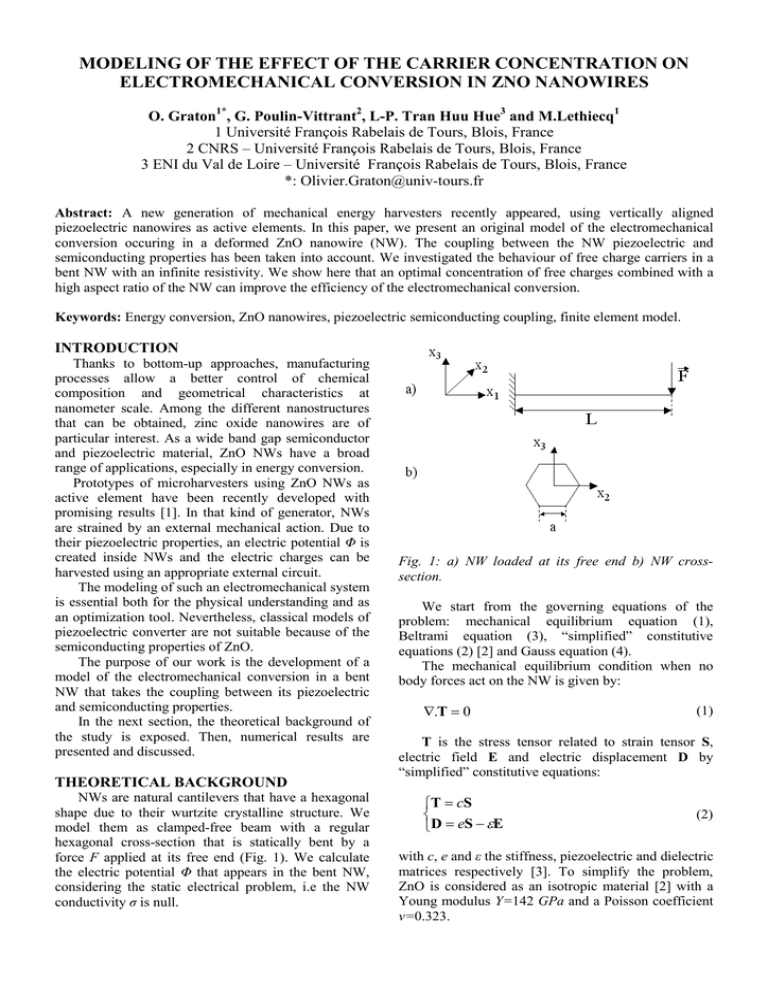
MODELING OF THE EFFECT OF THE CARRIER CONCENTRATION ON ELECTROMECHANICAL CONVERSION IN ZNO NANOWIRES O. Graton1*, G. Poulin-Vittrant2, L-P. Tran Huu Hue3 and M.Lethiecq1 1 Université François Rabelais de Tours, Blois, France 2 CNRS – Université François Rabelais de Tours, Blois, France 3 ENI du Val de Loire – Université François Rabelais de Tours, Blois, France *: Olivier.Graton@univ-tours.fr Abstract: A new generation of mechanical energy harvesters recently appeared, using vertically aligned piezoelectric nanowires as active elements. In this paper, we present an original model of the electromechanical conversion occuring in a deformed ZnO nanowire (NW). The coupling between the NW piezoelectric and semiconducting properties has been taken into account. We investigated the behaviour of free charge carriers in a bent NW with an infinite resistivity. We show here that an optimal concentration of free charges combined with a high aspect ratio of the NW can improve the efficiency of the electromechanical conversion. Keywords: Energy conversion, ZnO nanowires, piezoelectric semiconducting coupling, finite element model. INTRODUCTION Thanks to bottom-up approaches, manufacturing processes allow a better control of chemical composition and geometrical characteristics at nanometer scale. Among the different nanostructures that can be obtained, zinc oxide nanowires are of particular interest. As a wide band gap semiconductor and piezoelectric material, ZnO NWs have a broad range of applications, especially in energy conversion. Prototypes of microharvesters using ZnO NWs as active element have been recently developed with promising results [1]. In that kind of generator, NWs are strained by an external mechanical action. Due to their piezoelectric properties, an electric potential Φ is created inside NWs and the electric charges can be harvested using an appropriate external circuit. The modeling of such an electromechanical system is essential both for the physical understanding and as an optimization tool. Nevertheless, classical models of piezoelectric converter are not suitable because of the semiconducting properties of ZnO. The purpose of our work is the development of a model of the electromechanical conversion in a bent NW that takes the coupling between its piezoelectric and semiconducting properties. In the next section, the theoretical background of the study is exposed. Then, numerical results are presented and discussed. THEORETICAL BACKGROUND NWs are natural cantilevers that have a hexagonal shape due to their wurtzite crystalline structure. We model them as clamped-free beam with a regular hexagonal cross-section that is statically bent by a force F applied at its free end (Fig. 1). We calculate the electric potential Φ that appears in the bent NW, considering the static electrical problem, i.e the NW conductivity σ is null. Fig. 1: a) NW loaded at its free end b) NW crosssection. We start from the governing equations of the problem: mechanical equilibrium equation (1), Beltrami equation (3), “simplified” constitutive equations (2) [2] and Gauss equation (4). The mechanical equilibrium condition when no body forces act on the NW is given by: ∇.T = 0 (1) T is the stress tensor related to strain tensor S, electric field E and electric displacement D by “simplified” constitutive equations: T = cS D = eS − εE (2) with c, e and ε the stiffness, piezoelectric and dielectric matrices respectively [3]. To simplify the problem, ZnO is considered as an isotropic material [2] with a Young modulus Y=142 GPa and a Poisson coefficient ν=0.323. In the first equation of (2), the indirect piezoelectric effect is neglected, i.e we consider that stresses induced by E are small compared to those induced by F. This approximation is valid in our case because ZnO has relatively small piezoelectric coefficients. T must also satisfy Beltrami equation, which is a reformulation of the compatibility equation. It ensures that S derives from a displacement field: − ∇ 2T − 1 ∇∇(Tr (T)) = 0 1 +ν (3) Finally, the Gauss equation is given by: ∇.D = −QF (4) where QF is the free charge. Using (2) and (4), we reformulate Gauss equation as follows: ∇.(−εE) = −∇.(eS) − QF (5) ε 11S ∇ 2φ = QP − QF (6) We now have to determine the right terms of (6). QP is directly related to S and by the way to T. The stress tensor T in the bent NW is determined by solving (1) and (3). An analytical solution is found thanks to Saint Venant’s principle [4]. In that problem, we assume that T has the following form: T11 T12 T13 T = T12 0 0 T13 0 0 (7) Shear stresses T12 and T13 are obtained thanks to Bredt’s approximation [5], so T is fully determined: F(x1 − L) x3 IS T13 = F . IS (9) QF is the free charge in the NW. ZnO is a natural n-doped semiconductor due to defects in its crystal lattice that act like impurities. For simplicity of calculation, we consider only one shallow level donor Ed0=30 meV that represents Zn interstitial (Zni) [6]. QF is due to the presence of free electrons in the conduction band and ionized impurities on Ed0: QF = q ( N d+ − n) (10) with q the elementary charge. Free electrons concentration n and ionized impurities concentration Nd+ are calculated thanks to Fermi-Dirac statistics [7]: E F − EC ) kΘ Nd N +d = E + E d 0 − EC 1 + exp( F ) kΘ (11) where Nd is the Zni concentration, Nc the effective density of states in conduction band, k the Boltzmann constant, Θ the temperature and EF the Fermi level. EC is the conduction band edge of the NW. It is flat in the case of an undeformed NW. When the NW is bent, Φ and T deform the conduction band edge. This phenomenon is expressed as follow: EC = − qφ + ac 1 − 2ν Tr (T) Y (12) with ac the deformation potential of ZnO [8]. This expression is fundamental since it expresses the coupling piezoelectric and semiconducting properties. Since QF depends on Φ, (6) is a Poisson equation with a non-linear source term. We use the finite element method (FEM) to solve this problem. Numerical results and discussion T12 = 0 (8) −2 3 x3 (1+ν) 2 x3 − 4 3 a 3 + 4a2x − 3 a3 x3 3 3 9 3 x3 3 x3 e − 2νe F − 33 31 x3 = − e15 2 2 IS Y x 3 3 4Y a − 3 x3 n = N c exp( The first term of the right part of (5) represents the electric charge QP induced thanks NW piezoelectric properties [2]. Using the Maxwell-Faraday equation, we finally obtain the Poisson equation that gives the electric potential: T11 = − QP = −∇.(eS) = −∇.(ec−1T) . x + a.x − 1 .a 3 9 2 2.(a − 3 . x3 ) 3 3 3 2 3 where IS is the cross-section moment of inertia. We finally derive QP from T: We performed calculations for a 1µm length and 100 nm diameter NW bent by a load F = 0.2 µN surrounded by an insulating medium (air) at room temperature (Θ = 300 K). To stay in the small deformations approximation, we used a non-linearity mechanical criterion [5]: F≤ YI S 5 3dL (16) Results in Fig. 2 compare the electric potential Φ established in the half-length cross section of a lightly doped (Nd = 1e1010 cm-3) or moderately doped NW (Nd = 1e1017 cm-3). In the lightly doped case, Φ has a quasi-symmetric distribution, as it would be in a purely dielectric NW. The tensed side exhibits a positive potential Φ+ that reaches a maximum of 0.28 V whereas the compressed side shows a negative potential Φ- reaching –0.28 V. In the moderately doped case, Φ is no more symmetric and presents a maximum of only 0.04 V in the tensed side, while Φ is more preserved in the compressed side. Moreover, Nd+ is a fixed charge. It cannot freely move in the NW and because of its shallow level Ed0, almost all impurities are ionized (Nd+ ~ Nd). a) Fig. 3: Effect of electric potential Φ on conduction band edge Ec and free charge repartition. b) Fig. 4 presents the influence of the doping Nd and the NW aspect ratio L/d on Φ-. L and F are kept constant (L = 1 µm and F = 0.2 µN). We clearly see the existence of an optimal doping for which Φ- is maximized. For low values of Nd, we tend to the dielectric case, which is represented by dashed lines on the plot. For higher values of doping, even Φ- is screened and the electromechanical conversion is no longer efficient. Finally, for the same applied force, strains and stresses are increased in high aspect ratio NWs and lead to a higher electric charge QP induced by piezoelectric effect, thus to a higher Φ-. Fig. 2: Electric potential Φ in the half length cross section of a) a lightly doped NW (Nd=1e1010 cm-3) b) a moderately doped NW (Nd=1e1017 cm-3). This asymmetry comes from the fact that Φ is partially screened by free charges. (12) shows that Φ+ lowers the conduction band edge Ec, whereas Φ- raises it. This has a direct impact on the repartition of the free electrons; indeed, free electrons occupy in priority lower energy levels of the conduction band. Free electrons accumulate on the tensed side of the NW, whereas compressed side is depleted from free charge carriers. This phenomenon is illustrated in Fig 3. On compressed side, Φ- is partially screened by electric charges that come from ionized impurities Nd+. Fig. 4: Effect of the impurities concentration Nd on the electrical potential Φ for a NW with different aspect ratio L/d. Conclusion Numerical simulations give us a support for the physical understanding of the electromechanical conversion in ZnO NWs; they also indicate tendencies and are helpful to optimize the growth of those NWs. The energy conversion efficiency in a bent NW is maximized for high aspect ratio and optimal impurities concentration. Nevertheless, a challenge will be the modeling of the effect of the NW conductivity. A too high conductivity could result in an early internal discharge and dramatically diminish the electromechanical conversion efficiency. A mixed model of a conductive NW combining FEM and an equivalent circuit is under development. [3] [4] [5] [6] REFERENCES [1] [2] Wang X, Song J, Liu J, Wang Z L 2007 Direct-current nanogenerator driven by ultrasonic waves Science 316 102-105 Gao Y, Wang Z L 2007 Electrostatic potential in a bent piezoelectric nanowire. The fundamental theory of nanogenerator and nanopiezotronics Nano Lett. 7 (8) 2499-2505 [7] [8] Royer D, Dieulesaint E 1996 Ondes élastiques dans les solides (Paris, Masson) Timoshenko S, Goodier J N 1951 Theory of elasticity (New York, McGrow-Hill Book Company) Garrigues J 1999 Statique des poutres élastiques (Ecole Supérieure de Mécanique de Marseille) Look D C 2006 Progress in ZnO materials and devices J. Electron. Mater. 35 (6), 1299-1305 Vapaille A, Castagné R 1990 Dispositifs et circuits intégrés semiconducteurs (Paris , Dunod) Gao Y, Wang Z L 2009 Equilibrium potential of free charge carriers in a bent piezoelectric semiconductive nanowire Nano Lett. 9 (3) 11031110
