-
advertisement
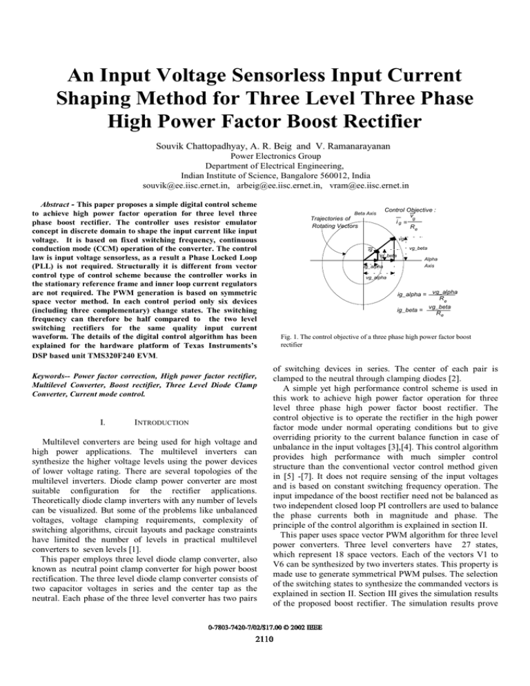
An Input Voltage Sensorless Input Current Shaping Method for Three Level Three Phase High Power Factor Boost Rectifier Souvik Chattopadhyay, A. R. Beig and V. Ramanarayanan Power Electronics Group Department of Electrical Engineering, Indian Institute of Science, Bangalore 560012, India souvik@ee.iisc.ernet.in, arbeig@ee.iisc.ernet.in, vram@ee.iisc.ernet.in Abstract - This paper proposes a simple digital control scheme to achieve high power factor operation for three level three phase boost rectifier. The controller uses resistor emulator concept in discrete domain to shape the input current like input voltage. It is based on fixed switching frequency, continuous conduction mode (CCM) operation of the converter. The control law is input voltage sensorless, as a result a Phase Locked Loop (PLL) is not required. Structurally it is different from vector control type of control scheme because the controller works in the stationary reference frame and inner loop current regulators are not required. The PWM generation is based on symmetric space vector method. In each control period only six devices (including three complementary) change states. The switching frequency can therefore be half compared to the two level switching rectifiers for the same quality input current waveform. The details of the digital control algorithm has been explained for the hardware platform of Texas Instruments’s DSP based unit TMS320F240 EVM. Keywords-- Power factor correction, High power factor rectifier, Multilevel Converter, Boost rectifier, Three Level Diode Clamp Converter, Current mode control. I. INTRODUCTION Multilevel converters are being used for high voltage and high power applications. The multilevel inverters can synthesize the higher voltage levels using the power devices of lower voltage rating. There are several topologies of the multilevel inverters. Diode clamp power converter are most suitable configuration for the rectifier applications. Theoretically diode clamp inverters with any number of levels can be visualized. But some of the problems like unbalanced voltages, voltage clamping requirements, complexity of switching algorithms, circuit layouts and package constraints have limited the number of levels in practical multilevel converters to seven levels [1]. This paper employs three level diode clamp converter, also known as neutral point clamp converter for high power boost rectification. The three level diode clamp converter consists of two capacitor voltages in series and the center tap as the neutral. Each phase of the three level converter has two pairs Control Objective : v g ig = Re Beta Axis Trajectories of Rotating Vectors vg vg_beta ig ig_beta Alpha Axis ig_alpha vg_alpha ig_alpha = vg_alpha Re ig_beta = vg_beta Re Fig. 1. The control objective of a three phase high power factor boost rectifier of switching devices in series. The center of each pair is clamped to the neutral through clamping diodes [2]. A simple yet high performance control scheme is used in this work to achieve high power factor operation for three level three phase high power factor boost rectifier. The control objective is to operate the rectifier in the high power factor mode under normal operating conditions but to give overriding priority to the current balance function in case of unbalance in the input voltages [3],[4]. This control algorithm provides high performance with much simpler control structure than the conventional vector control method given in [5] -[7]. It does not require sensing of the input voltages and is based on constant switching frequency operation. The input impedance of the boost rectifier need not be balanced as two independent closed loop PI controllers are used to balance the phase currents both in magnitude and phase. The principle of the control algorithm is explained in section II. This paper uses space vector PWM algorithm for three level power converters. Three level converters have 27 states, which represent 18 space vectors. Each of the vectors V1 to V6 can be synthesized by two inverters states. This property is made use to generate symmetrical PWM pulses. The selection of the switching states to synthesize the commanded vectors is explained in section II. Section III gives the simulation results of the proposed boost rectifier. The simulation results prove 0-7803-7420-7/02/$17.00 © 2002 IEEE 2110 PWM Converter Unit Vo C L Input a vga phases b vgb c vgc Swa1 Swb1 Rc Vo Swc1 C L X L igc igb iga Swa2 Swb2 Swc2 R Y Swb3 Swa3 Measurement of phase currents Vo/2 Swc3 Phase X C Swa4 Swb4 Rc Swc4 X 1 0 0 C Swa1 Swa2 Swa3 Swa4 Swb1 Swb2 Swb3Swb4 Swc1 Swc2 Swc3 Swc4 Y Controller generating switching pulses for the PWM converter DC Voltage Sensing State 1 0 -1 (c) (b) (a) Y 2 1 0 Fig. 2. (a) Three phase three level Boost rectifier circuit and control schematic. (b) Naming convention of switches in each phase. (c) The definition of ‘State’s based on the switch combination . vgα i β axis Phase B Axis V10 (-1,+1,-1) V9 (0,+1,-1) 3L 2 vo Qα α Axis Boost gα Sector '4' V11 Sector '5' V3 (-1,+1,0) -1,0,-1/0,+1,0 R Rectifier Dα current processing clk S Q R ig αr sf(i) R Q Carrier Gen + voltage regulator 3L 2 vg β Vm V14 (-1,-1,+1) Phase C Axis Rectifier D β current processing igβr clk S Q R sf(i) V16 (+1,-1,+1) the validity of the control algorithm. In general the present work offers a simple controller with cost effective three level three phase boost rectifier for high voltage applications. R Q Comparator vc V15 (0,-1,+1) Fig. 4. Definition of voltage vectors and the corresponding sectors Q β β Axis Boost gβ V0 Sector '9' Sector '10' Vref vo - i Sector '1' α axis +1,0,0/0,-1,-1 Phase A V1 V18 (+1,-1,-1) Axis Sector '12' -1,-1,0/0,0,+1 +1,0,+1/0,-1,0 V6 V5 V17 (+1,-1,0) V13 Sector '11' (-1,0,+1) Sector '8' Comparator vc Sector '2' V7 (+1,0,-1) V2 +1,+1,0/0,0,-1 Sector '6' V4 V12 (-1,+1,+1) 0,+1,+1/-1,0,0 Sector '7' V8 (+1,+1,-1) Sector '3' Carrier Gen Fig. 3. Functional representation of three phase high power factor boost rectifier with two independent single phase rectifiers in current mode control structure. II. CONTROLLER We can define the control objective of a three phase high power factor Boost rectifier, as ig = 2111 vg Re (1) Three possible control objectives of resistor emulator type current mode controller vg/Re (a) peak current control V10 V8 igrpk = vg/Re V8 Sector '2' A Sector '5' B V11 V7 V2 V3 Sector '2' N V7 V2 = vg/Re (b) average current control V13 Sector '8' igrav = vg/Re V6 V5 V17 D Sector '11' C V16 V14 vg/Re (c) Fig. 7. Mapping of A,B,C,D vectors into N of Sector 2 for solution of T1 and T2 (refer table II) end of the period current control igre = vg/Re Definition of end of the period current control in discrete domain : d[n] = 1- (Rs.igre[n-1]/ Vm) TABLE II Vectors in sectors 2,5,8 and 11 igre[n-1] : current at the end of (n-1)thperiod igrb[n] : current at the beginning of nth period igrb[n] = igre[n-1] Sector e[n-2] vm /Rs vm /Rs igre[n-1] d[n] d[n-1] (d) Ts Ts Fig. 5. Discrete version of resistance emulator type current mode controller A v1 A v2 A vm 2 V7 V8 V2 5 V11 V10 V3 8 V13 V14 V5 11 V17 V16 V6 V10 V9 Sector '4' L V8 Sector '3' K V9 Sector '3' O V2 V2 V3 V8 = V11 V7 V7 Q V4 V12 V18 V1 R V12 = V1 V18 V14 S Sector '12' Sector '7' J M Sector '9' Sector '10' M P V6 V5 Sector '1' Sector '1' Sector '6' V16 V15 V17 V13 Fig. 8. Mapping of K,L,M,J vectors into N of Sector 2 for solution of T1 and T2 (refer table III) Fig. 6. Mapping of P,Q,R,S vectors into M of Sector 1 for solution of T1 and T2 (refer table I) TABLE III Vectors in sectors 3,4,9 and 10 TABLE I Vectors in sectors 1,6,7 and 12 Sector Sector 1 A v1 V7 A v2 A vm V18 V1 6 V11 V12 V4 7 V13 V12 V4 12 V17 V18 V1 2112 A v1 A v2 A vm 3 V9 V8 V2 4 V9 V10 V3 9 V15 V14 V5 10 V15 V16 V6 any arbitrary initial assumption of sector V o (1−d ) (5) i gr = Re V o is the regulated output of the overall rectifier. i g r and 6 5 4 3 2 1 7 8 9 10 11 12 i gr are obtained by rectifying i g . and i g respectively. Conceptually this is eqivalent to two current sources charging the same capacitor for voltage output. The control structure is also shown in Fig.3. In continuous time domain, i g r and i gr can be made to represent peak current, average current , or end of the period current of the inductor in every switching period T s . This is shown in Fig. 5(a) ,5(b) and 5(c) respectively. Fig.2 (a) gives the circuit and control schematic of three phase three level boost rectifier. The naming convention of the switches in each phase are according to Fig.2(b) and Fig.2(c) gives the definition of ‘State’s based on the valid switch combination. Our definition of voltage vectors and the corresponding sectors are shown in Fig.4. However, in discrete implementation, current is sampled only once in a switching period. So, unless the sampling instant in a period is varied [4], the control objectives shown in Fig.5(a) or 5(b) can not be implemented. In contrast, Fig.5(c) is ideal for digital implementation, because the sampling instant can be kept fixed at the beginning of every switching period. We can calculate the duty ratios d [n] and d [n] from expressions Actual sector location of the input voltage vector Fig. 9. Sequence of sector change to be followed to eventually synchronize with the location of the input voltage vector. underflow interrupt CMP1 SCMP1 SCMP3 0 1 1 1 0 0 1 Ts/2 Sampling Period 1 0 0 0 1 Tm T2 T1 Tm 4 2 2 4 Ts, n-1 Calculation cycle n t ) = (1 − i gr [n]R s Vm ) (6) d [n] = (1 − i gre [n−1]R s Vm ) = (1 − i gr [n]R s Vm ) (7) VoR s , where R e is the emulated resistance of the rectifier. The ( ) above a variable indicates a space phasor. This control objective is shown in Fig. 1. If we take components along and axes, which are stationary and orthogonal to each other, the control objective can be expressed in terms of two scalar equations i g = vg Re (2) ig = vg Re (3) as shown in Fig. 1. This is equivalent to control of two single phase Boost rectifiers, one in axis and the other in axis, as shown in Fig.3. Let us assume here that the duty ratios d and d of these two switches Q and Q can be independently controlled. So, we can write, V o (1−d ) Re i gre [n−1]R s Vm Ts, n Calculation cycle n+1 Fig.10 Symmetric PWM generation in the Event manager module of DSP TMS320F240. In each sector out of six independent PWM signals only three signals switch. For example in Sector 1 XA (CMP1), YB (SCMP1) and YC(SCMP3) change states and YA(high),XB(low) and XC(low) remain clamped throughout the periodT s . i gr = d [n] = (1 − after replacing R e by V m in (4) and (5). The suffix e indicates that the current is sampled at the end of the period. It should be noted that the current at the end of period [n − 1] is same as the current at the beginning of period [n] . This is shown in Fig.5(d). Here, R s is the current sensing resistance. However, we need to satisfy (6) and (7) simultaneously in every switching period. So, from d [n] and d [n] , we have to determine the time duration T 1 [n] and T 2 [n], for the two active vectors A v1 and A v2 respectively, to effectively produce the same volt-sec on each axis as demanded by the independent controllers. The remaining time T o [n] of the period should be used for the null vector A vo . From Fig.6, it can be noted that if the active vectors A v1 and A v2 for sectors 1, 6, 7 and 12 are identified as in Table I, then the corresponding time T 1 [n] and T 2 [n], needed for synthesis of any vector (P, Q, R or S) with an angle with respect to the axis of the segment, can be obtained by solving the following simultaneous equations. (4) 2113 ( 3 2 ). 3 2 ( 3 2 ) 12 T 1 [n] = (1 − d [n])T s T 1 [n] + T 2 [n] = (1 − d [n])T s (8) (9) TABLE IV i g . and i g TABLE V Full compare unit of TMS320F240 in each sector Sector i gr [n] i gr [n] 1 i g [n] i g [n] sec tor CMP1 for signal Xa 2 i g [n] i g [n] 1 3 i g [n] 2 i g [n] T x = (T s − T 1 − T 2 )/4 4 i g [n] i g [n] T x = (T s − T 1 − T2 )/4 3 5 − i g [n] i g [n] 4 6 − i g [n] 7 −i g [n] −i g [n] 8 −i g [n] − i g [n] −i g [n] 9 10 ig [n] i g [n] 11 i g [n] 12 g [n] 5 6 7 −i g [n] −i g [n] 8 3 2 ). 3 2 ( 3 2 ). 12 T 1 [n] + ( 0 0 T x + T 1 /2 T x + T 1 /2 0 T x = (T s − T 1 − T 2 )/4 T s /2 T x + T 2 /2 T x + T 2 /2 + T 1 /2 T s /2 T s /2 T x + T 2 /2 + T 1 /2 T s /2 T x + T 2 /2 + T 1 /2 T x + T 1 /2 11 T x = (T s − T 1 − T 2 )/4 12 T x = (T s − T 1 − T 2 )/4 ( ).T 1 [n] + ( 3 2 ).T 2 [n] = (1 − d [n])T s T x = (T s − T 1 − T2 )/4 T x = (T s − T 1 − T 2 )/4 T x + T 1 /2 T s /2 T s /2 0 T s /2 T s /2 0 T s /2 0 T s /2 (10) (11) TABLE VI Simple compare unit of TMS320F240 (12) sector 3 2 T x = (T s − T 1 − T 2 )/4 T x + T 2 /2 −i g [n] = (1 − d [n])T s T x + T 1 /2 + T 2 /2 T s /2 For sectors 3, 4, 9 and 10 ,as shown in Fig.8, Table III gives the selection of vectors. The following simultaneous equations can be used to solve for T 1 [n] and T 2 [n]. 1 2 T 2 [n] 10 ).T 2 [n] = (1 − d [n])T s T s /2 −i g [n] T 1 [n] + ( 12 ).T 2 [n] = (1 − d [n])T s 3 2 CMP3 for signal Xb 9 For sectors 2, 5, 8 and 11 , as shown in Fig.7, Table II gives the selection of vectors. The following simultaneous equations can be used to solve for T 1 [n] and T 2 [n]. ( CMP2 for signal Ya (13) It can be seen that input voltage need not be sensed for computation of T 1 [n] and T 2 [n]. However the sector information should be known for appropriate selection of active vectors. This controller implements self-synchronization of the converter switching with respect to line voltage based on the following logic: as long as the sector selection is correct , the and axis modulators will produce duty ratios less than 1, i.e, d [n] < 1 or d[n] < 1. Similarly T 1 > 0 and T 2[n] > 0 have to be satisfied for the modulator to operate in the unsaturated region. When any one of these conditions are violated , the next sector in sequence is chosen, as shown in Fig.9. This sector change can take place in the same switching cycle in which it had saturated because of incorrect selection of vectors. After that the modulator will recalculate the duty ratios, which won’t saturate now as the sector selection is correct. In this implementation of the three level switching we will not use any zero vector , instead the 2114 1 2 3 4 5 6 7 SCMP1 for signal Yb SCMP2 for signal Xc SCMP3 for signal Yc T x + T 2 /2 T s /2 0 T s /2 T x + T 1 /2 + T 2 /2 T x + T 1 /2 + T 2 /2 0 0 T s /2 T x + T 1 /2 + T 2 /2 T s /2 T x + T 1 /2 + T 2 /2 0 0 T s /2 T x + T 2 /2 T x + T 1 /2 0 T x = (T s − T 1 − T 2 )/4 0 0 T x = (T s − T 1 − T 2 )/4 8 T x + T 2 /2 9 T x + T 1 /2 + T 2 /2 10 T x + T 1 /2 + T 2 /2 11 T x + T 1 /2 + T 2 /2 12 T x + T 1 /2 + T 2 /2 T x = (T s − T 1 − T 2 )/4 T x = (T s − T 1 − T 2 )/4 T x + T 1 /2 T s /2 0 0 0 0 T x + T 2 /2 Vo=700V 40 Vo=700V Po=3.3Kw Po=10Kw 40 0.1*Vga 0.1Vga 30 30 Sector 20 20 Sector 10 10 0 0 -10 -10 Igc Igb Iga -20 -20 -30 -30 -40 -40 0 0.005 0.01 0.015 0.02 0.025 0.03 0.035 0.04 Igc 0 Iga 0.005 Igb 0.01 0.015 0.02 Vo=700V Po=10Kw Igb Vo=700V 40 40 Igc 30 0.03 0.035 0.04 (b) (a) Iga 0.025 time time Po=10Kw 30 20 20 10 10 0 0 -10 -10 -20 -20 -30 -30 0.1*Vga Sector Igc Iga Igb 0,1*Vga -40 -40 0 0.005 0.01 0.015 0.02 0.025 0.03 0.035 0.04 0 0.005 0.01 0.015 0.02 0.025 0.03 0.035 0.04 time time (d) (c) Fig. 11 (a) and(b) show input phase voltages and currents at load 3.3Kw and 10Kw respectively. The sector change sequence is also shown. (c) and (d) show input phase voltages and currents at 70% and 110% of the rated input voltage for 10Kw load. 1.2 1.2 1 CMP1-XA 1.2 1 1 0.8 0.8 SCMP2-XC 0.8 CMP3-YB 0.6 0.6 CMP2-YA 0.4 0.4 0.2 0.2 0.6 SCMP1-XB 0.4 SCMP3-YC 0.2 0 0 0 -0.2 0 -0.2 0 -0.2 0 0.005 0.01 0.015 0.02 0.025 0.03 0.035 0.04 0.005 0.01 0.015 0.02 time time (b) (a) Ts Fig.12 (a),(b), and (c) show the normalized profile ( 2 Table VI over the line cycle. 0.025 0.03 0.035 0.04 0.005 0.01 0.015 0.02 0.025 0.03 0.035 0.04 time (c) isequivalentto1) of the compare register entries for the switches XA,YA,XB,YB,XC and YC as listed in 2115 effective volt-sec will be synthesized by A v2 , now switched for duration T2, and A vm , switched for duration T m = (T s − T 1 − T 2 ) T 2 = 2T 2 − T s + T 1 (14) T m = 2(T s − T 1 − T 2 ) (15) load 3.3Kw and 10Kw respectively. The sector change sequence is also shown. Fig.11 (c) and (d) show input phase voltages and currents at 70% and 110% of the rated input voltage for 10Kw load. Fig.12 (a),(b), and (c) show the Ts normalized profile ( 2 isequivalent to1) of the compare register entries as listed in Table V and Table V1 over a line cycle for the switches XA,YA,XB,YB,XC and YC. IV. In each sector of Fig. 4, A vm can be identified as the middle level vector , as specified in Table I, II and III. It can be produced by two alternative combinations of switching states . It will be shown in later part of this discussion that by effectively using this property of the middle level vector we can generate symmetric PWM pulses from the event manager module of the DSP TMS320F240. Here we should explain the current processing function of the modulator. First, the two phase currents i ga [n] and i gb [n] are sensed and converted to i g [n] and i g [n] by standard three phase to two phase transformation. However, the modulators work on DC quantities, so based on the sector information, we generate i gr [n] and i gr [n] , as shown in Table 1V, and use them for calculation of duty ratios. In any phase of the converter, if we do not consider the effect of dead time in the switching signals, then it can be seen from Fig.2(b) that only two of the four switching signals have to be independently controlled. The switching states produced by the combination of signals for these switches ,(1=ON,0=OFF), are defined in Table 1. So, in each switching period, the TMS320F240 based digital controller has to generate six independent PWM signals corresponding to the previously computed T 1, T 2 and T m values. The ‘Event Manager Module’ of TMS320F240 has two ‘Compare Unit’s , each consisting of three compare registers , that are loaded with values given by Table V and Table VI. Each compare unit is clocked by the internal timer circuit, Timer 1 in this case, at the required frequency. In this implementation the timer is configured to work in ‘continuous up-down’ counting mode. Each cycle of control calculations are initiated by the timer ‘underflow interrupt’. It can be observed from Table V and Table VI that only three of the six signals change states in a control period. The symmetrical PWM generation procedure for sector 1 is shown in Fig 10 as an example. III. SIMULATION RESULTS This paper describes a discrete current mode control algorithm that can performs high power factor operation for a three phase three level Boost rectifier. The salient features of this controller are : (1) No input voltage sensing is required, as switching pulses get self-synchronized with the line frequency, (2) No need to use PLL, as the controller works in stationary reference frame, (3) Two decoupled fixed frequency current mode controllers are used to generate the equivalent ON and OFF durations for shaping currents in two orthogonal axes , (4) A combined switching strategy is developed in the form of space vectors to simultaneously satisfy the timing requirements of both the current mode controllers in a control period. (5) The PWM signals are symmetric , requires only three switches (also the complementary devices) to change states in a control period and can be implemented in a general purpose DSP like TMS320F240. The switching frequency therefore can be half compared to the two level rectifiers for the same quality of input current wave form. In conclusion, it can be said that, this method of control of three phase three level high power factor boost rectifier provides comparable or better performance over existing methods with a much simpler control structure. REFERENCES [1] [2] [3] [4] [5] The proposed controller is simulated on MATLAB-SIMULINK (version 5.3) software platform. The nominal rating of the three phase Boost rectifier is chosen to be 10Kw, 415Vac, 700Vdc .The inductance/phase is 3mH . The control loop period is T s = 100Sec , so the switching frequency of the semiconductor devices is 2.5KHz . Under rated input voltage condition and at regulated 700V output, Fig. 11 (a) and(b) show input phase voltages and currents at CONCLUSION [6] [7] [8] 2116 Jih-Sheng Lai and Fang Zheng Peng, “Multilevel Converters -A new breed of power converters,” IEEE Transactions on Industry Applications, vol .32, no .3, pp 509-517, May/June 1996. Akira Nabae, I. Takahashi and H. Akagi, “A new neutral point clamped PWM inverterrs,” IEEE Transactions on Industry Applications, vol.7, no. 5, pp 518 -523, Sept/Oct 1981. Souvik Chattopadhyay and V. Ramanarayanan , "Digital implementation of a line current shaping algorithm for three phase high power factor Boost rectifier without input voltage sensing,,” Proc. of APEC’01, pp. 592-600, 2001 S.Buso,P.Mattavelli, L.Rossetto and G.Splazzi, “ Simple Digital Control Improving Dynamic Performance of Power Factor Preregulators,” IEEE Transactions on Power Electronics , Vol. 13, No. 5, Sept 1998. H. S. Kim, H. S. Mok, G. H. Choe, D. S. Hyun and S. Y. Choe “Design of Current Controller for 3-Phase PWM Converter with unbalanced input Voltage,” Proc. of IEEE PESC Conference, 1998, pp503-509, 1998 Ana Vladan Stankovic and Thomas A. Lipo, “ A novel control method for input output harmonic elimination of the PWM Boost type rectifier under unbalanced operating conditions,” IEEE Transactions on Power Electronics, vol. 16, no. 5, pp. 603-611, Sept. 2001. P.Rioual, H.Pouliquen and J.P.Louis, “Regulation of a PWM rectifier in the unbalanced network state,” Proc. IEEE-PESC Conference, pp.641-649 , 1993. TMS320C24x DSP Controllers Peripheral Library and Specific Devices Reference Set - Volume 2, Literature Number : SPRU161B December 1997.


