Technical Note 10481
Effective December 2015
Supersedes March 2007
Inductor selection
for SEPIC designs
Inductor selection for SEPIC designs
Overview
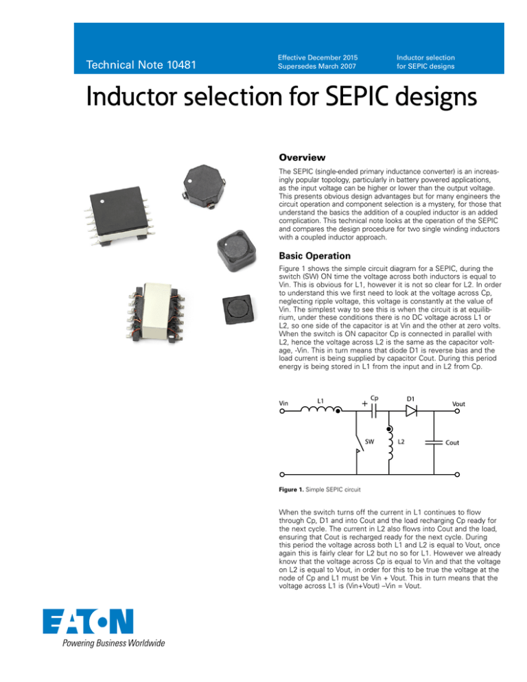
The SEPIC (single-ended primary inductance converter) is an increasingly popular topology, particularly in battery powered applications,
as the input voltage can be higher or lower than the output voltage.
This presents obvious design advantages but for many engineers the
circuit operation and component selection is a mystery, for those that
understand the basics the addition of a coupled inductor is an added
complication. This technical note looks at the operation of the SEPIC
and compares the design procedure for two single winding inductors
with a coupled inductor approach.
Basic Operation
Figure 1 shows the simple circuit diagram for a SEPIC, during the
switch (SW) ON time the voltage across both inductors is equal to
Vin. This is obvious for L1, however it is not so clear for L2. In order
to understand this we first need to look at the voltage across Cp,
neglecting ripple voltage, this voltage is constantly at the value of
Vin. The simplest way to see this is when the circuit is at equilibrium, under these conditions there is no DC voltage across L1 or
L2, so one side of the capacitor is at Vin and the other at zero volts.
When the switch is ON capacitor Cp is connected in parallel with
L2, hence the voltage across L2 is the same as the capacitor voltage, -Vin. This in turn means that diode D1 is reverse bias and the
load current is being supplied by capacitor Cout. During this period
energy is being stored in L1 from the input and in L2 from Cp.
Figure 1. Simple SEPIC circuit
When the switch turns off the current in L1 continues to flow
through Cp, D1 and into Cout and the load recharging Cp ready for
the next cycle. The current in L2 also flows into Cout and the load,
ensuring that Cout is recharged ready for the next cycle. During
this period the voltage across both L1 and L2 is equal to Vout, once
again this is fairly clear for L2 but no so for L1. However we already
know that the voltage across Cp is equal to Vin and that the voltage
on L2 is equal to Vout, in order for this to be true the voltage at the
node of Cp and L1 must be Vin + Vout. This in turn means that the
voltage across L1 is (Vin+Vout) –Vin = Vout.
Inductor selection for SEPIC designs
Technical Note 10481
Effective December 2015
Inductor Selection
Output inductor L2
First, let us look at the selection of two separate inductors for L1 and
L2 in the following example:
Irms= Iout= 1 A
Iripple= (4.5 x 1.69 x 10-6)/22 x 10-6 = 0.346 A
Ipeak= 1 + (0.5 x 0.346) = 1.173 A
Input voltage (Vin): 2.8 V to 4.5 V
Output (Vout, Iout): 3.3 V, 1 A
Switching Frequency (Fs): 250 kHz
Efficiency: 90%
A 22 μH, 1 A rms & 1.173 A pk rated inductor is required. For
simplicity the Eaton DR73-220-R inductor could be selected for the
L2 inductor also.
Calculating the duty cycle (D);
Coupled inductor selection
D = Vout/(Vout+ Vin)
The worst case condition for inductor ripple current is at maximum
input voltage so;
D = 3.3/(3.3 + 4.5) = 0.423
When calculating the value for a coupled inductor keep in mind that
all the current is effectively flowing in one inductor and that if the two
windings are closely coupled the ripple current will be split equally
between them.
Normally, the output inductor is sized to ensure that the inductor
current is continuous at minimum load and that the output voltage
ripple does not affect the circuit that the converter is powering. In
this case we will assume a 20% minimum load thus allowing a 40%
peak to peak ripple current in the output inductor L2.
Calculating the inductance value:
L = V x dt/di
Calculating the value of L2;
From our earlier example the output ripple current needs to be
0.4 A pk-pk, so now we calculate for 0.8 A pk-pk as the ripple current is split between the two windings.
V = L x di/dt.
L = 4.5 x (1.69 x 10-6/0.8) = 9.5 µH
Where V is the voltage applied to the inductor, L is the inductance, di
is the inductor peak to peak ripple current and dt is the duration the
voltage is applied for.
Using a coupled inductor allows the required inductance to be
halved. It is also important to note that because the two winding are
on the same core they must be the same value. If they are not the
voltage across each winding will not be equal and Cp will act as a
short circuit to the difference.
L = V x dt/di
dt = 1/Fs x D
dt = 1/(250 x 103) x 0.423 = 1.69 µs
V = Vin during the switch ON time so;
L2 = 4.5 x (1.69 x 10-6/0.4)
L2 = 19 µH
Using the nearest preferred value would lead to the selection of a
22 µH inductor. It is common practice to select the same value for
both input and output inductors in SEPIC designs although when two
separate parts are being used it is not essential.
Input inductor L1;
Irms= (Vout x Iout)/(Vin (min) * efficiency)
Irms= (3.3 x 1)/(2.8 x 0.9) = 1.31 A
Ipeak= Irms+ (0.5 x Iripple)
Although worst case ripple current is at maximum input voltage
the peak current is normally highest at the minimum input voltage.
Recalculate D and dt using minimum input voltage.
D=3.3/(3.3 + 2.8)= 0.540
dt=1/(250 x 103) x 0.540= 2.2 µs
Iripple= (V x dt)/L
Iripple= (2.8 x 2.2 x 10-6)/22 x 10-6= 0.28 A
Ipeak= 1.31 + (0.5 x 0.28) =1.45 A
A 22 μH, 1.31 A rms and 1.45 A pk rated inductor is required.
One such example would be the Eaton DR73-220-R inductor which is
7.5mm square and 3.5mm high with 1.62 A rms and 1.67 A pk
current rating.
Continuing with the example using an inductance value of 10 µH;
calculate the worst case peak current requirement.
Input inductor rms current = 1.31 A
Output inductor rms current = 1 A
Ipeak= Iin+ Iout+ (0.5 x Iripple)
Iripple= (2.8 x 2.2 x 10-6)/10 x 10-6= 0.62A
Ipeak= 1.31 + 1 + (0.5 x 0.62) = 2.62A @ minimum input voltage
A 10 μH coupled inductor with 2.31 A rms and 2.62 A pk current
ratings is required, for example the Eaton DRQ74-100-R Inductor
which is 7.5 mm square and 4.35 mm high.
Conclusion:
Using a coupled inductor takes up less space on the PCB and tends
to be lower cost than two separate inductors. It also offers the option
to have most of the inductor ripple current flow in either the input
or the output. This is achieved by using a winding construction that
positions most of the leakage inductance in one winding, this will
cause most of the ripple current to appear in the opposite winding.
By doing this the need for input filtering can be minimized or the output ripple voltage can be reduced to very low levels when supplying
sensitive circuits.
Eaton offers a number of coupled inductor options including the SDQ
and DRQ family of shielded drum inductors, the Econo-Pac, Octa-Pac
, and Octa-Pac plus range of toroid inductors and the Versa-Pac configurable inductor/transformer with inductance values from 0.30 μH
to over 4.72 mH in a wide variety of sizes and current ranges.
Eaton
1000 Eaton Boulevard
Cleveland, OH 44122
United States
www.eaton.com/elx
© 2015 Eaton
All Rights Reserved
Printed in USA
Publication No. 10481
December 2015
Eaton is a registered trademark.
All other trademarks are property
of their respective owners.
