6.012 - Electronic Devices and Circuits -
advertisement
6.012 - Electronic Devices and Circuits - Take Home Diagnostic Exercise
The four problems in this exercise deal with material you will use in 6.012 from the
prerequisite courses. Give yourself one hour to work it. Solutions will be distributed at
the next recitation and you can then judge for yourself which material you need to review.
Problem 1 - Basic linear circuit analysis
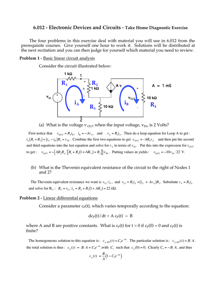
Consider the circuit illustrated below:
1 kΩ
1
+
R1
vIN
vA
+
-
R2
A vA
1 kΩ
-
iA
vOUT
R3
10 kΩ
A = 1 mS
+
iB
10 kΩ
-
R4
2
(a) What is the voltage v OUT when the input voltage, vIN, is 2 Volts?
First notice that
vOUT = R4 iB , iB = −Av A , and
v A = R2iA . Then do a loop equation for Loop A to get :
iA ( R1 + R2 ) + (iA − iB ) R3 = v IN . Combine the first two equations to get vOUT = -AR4 v A
and then put the second
and third equations into the last equation and solve for v A in terms of v IN . Put this into the expression for vOUT
to get :
€
vOUT = −{ AR2 R4 [ R1 + R2 (1 + AR 3 ) + R3 ]}v IN . Putting values in yields :
vOUT = −10v IN 22 V.
(b) What is the Thevenin equivalent resistance of the circuit to the right of Nodes 1
and 2?
The Thevenin equivalent resistance we want is v12 iA , and v12 = R2iA + (iA + Av A ) R3 . Substitute v A = R2iA
and solve for R T : RT = v12 iA = R2 + R3 (1+ AR2 ) = 22 kΩ.
Problem 2 - Linear differential equations
€
Consider a parameter cP(t), which varies temporally according to the equation:
dcP(t)/dt + A cP(t) = B
where A and B are positive constants. What is cP(t) for t > 0 if cP(0) = 0 and cP(t) is
finite?
The homogeneous solution to this equation is : c p, HS (t) = C1e−At . The particular solution is : c p, HS (t) = B A.
the total solution is thus : c p (t) = B A + C1e−At ,with C1 such that c p (0) = 0. Clearly C1 = − B A, and thus
c p (t) =
€
B
(1− C1e−At )
A
Problem 3 - Linearization about an operating point
Consider the non-linear two-terminal electronic device, D, illustrated below on
the left. The current through the device, iD(t), is related to the voltage across its
terminals, vAB(t), by the equation, iD(t) = B (vAB + C vAB3), where B = 10-3 A/V and C =
4 V-2.. There is no charge or flux storage associated with this device.
iD
A
+
Non-linear
two-terminal
device, D
B
-
R
i d
a
+
v ab
vAB
-
b
A linear equivalent circuit for the device D valid for small signal operation about a
bias point, vAB = VAB, is shown to the right. What is R for the bias point VAB = 2V?
R=
1
∂i
, where gd ≡ D
gd
∂v AB
[
]
2
. We find : gd = B(1 + 3CVAB
). Thus : R = 1 B(1 + 3CVAB2 ) = 40 Ω.
v AB =VAB
Problem 4 - Simple electrostatics
€
In a certain sample of material the electric field, E(x,y,z), varies only in the xdirection, i.e., E(x,y,z) = E(x), where E(x) is shown below. The dielectric constant, ε, is
uniform throughout the sample with a value of 10-10 coul/V-cm.
2
E(x) [V/cm]
10
-3
-2
-1
1
-10
2
3
x [µm]
2
On the axes provided below, sketch and dimension the net charge distribution in
this sample.
ρ(x) = ε
dE
= Q * [δ (1µm) - δ (-1µm)], where Q* = (10−10 coul/V - cm)(1.5 x 10 2 V/cm) = 1.2x10⁻¹² coul /cm 2 .
dx
Q*
€
-3
-2
-1
-Q*
1
2
3
x [µm]
MIT OpenCourseWare
http://ocw.mit.edu
6.012 Microelectronic Devices and Circuits
Fall 2009
For information about citing these materials or our Terms of Use, visit: http://ocw.mit.edu/terms.
