6.012 - Electronic Devices and Circuits
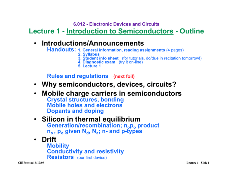
Lecture 1 - Introduction to Semiconductors - Outline
• Introductions/Announcements
Handouts:
1. General information, reading assignments (4 pages)
2. Syllabus
3. Student info sheet (for tutorials, do/due in recitation tomorrow!)
4. Diagnostic exam (try it on-line)
5. Lecture 1
Rules and regulations (next foil)
• Why semiconductors, devices, circuits?
• Mobile charge carriers in semiconductors
Crystal structures, bonding
Mobile holes and electrons
Dopants and doping
• Silicon in thermal equilibrium
Generation/recombination; nopo product
no , po given Nd, Na; n- and p-types
• Drift
Mobility
Conductivity and resistivity
Resistors (our first device)
Clif Fonstad, 9/10/09
Lecture 1 - Slide 1
Comments/Rules and expectations
Recitations: They re-enforce lecture.
They present new material.
They are very important.
Tutorials:
They begin Monday, September 14.
Assignments will be posted on website.
Homework: Very important for learning; do it!!
Cheating: What you turn in must be your own work.
While it is OK to discuss problems with others, you should
work alone when preparing your solution.
Reading assignment (Lec. 1)
Chapter 1 in text*
Chapter 2 in text
* "Microelectronic Devices and Circuits" by Clifton Fonstad
http://dspace.mit.edu/handle/1721.1/34219
Clif Fonstad, 9/10/09
Lecture 1 - Slide 2
SEMICONDUCTORS: Here, there, and everywhere!
• Computers, PDAs, laptops,
Silicon (Si) MOSFETs, Integrated Circuits (ICs),
anything “intelligent”
CMOS, RAM, DRAM, flash memory cells
• Cell phones, pagers, WiFi
Si ICs, GaAs FETs, BJTs
• CD players, iPods
AlGaAs and InGaP laser diodes, Si photodiodes
• TV remotes, mobile terminals
Light emitting diodes
• Satellite dishes
InGaAs MMICs
• Optical fiber networks
InGaAsP laser diodes, pin photodiodes
• Traffic signals, car
GaN LEDs (green, blue)
taillights, dashboards
InGaAsP LEDs (red, amber)
• Air bags
Si MEMs, Si ICs
They are very important, especially to EECS types!!
They also provide:
a good intellectual framework and foundation, and
a good vehicle and context
with which
to learn about modeling physical processes,
and
to begin to understand electronic circuit analysis and design.
Clif Fonstad, 9/10/09
Lecture 1 - Slide 3
Silicon:
our default example and our main focus
Atomic no. 14
14 electrons in three shells: 2 ) 8 ) 4
i.e., 4 electrons in the outer "bonding" shell
Silicon forms strong covalent bonds with 4 neighbors
Si bonding
configuration
Silicon crystal ("diamond" lattice)
Figure by MIT OpenCourseWare.
Silicon crystal
("diamond" lattice)
Clif Fonstad, 9/10/09
Lecture 1 - Slide 4
Intrinsic silicon - pure, perfect, R.T.:
Electron
energy
• All bonds filled at 0 K, po = no = 0
Conducting
states
Si
-
Eg
+
• At R. T., po = no = ni = 1010 cm-3
• Mobile holes (+) and mobile electrons (-)
• Compare to ≈ 5 x 10²² Si atoms/cm3
Clif Fonstad, 9/10/09
Eg ≈ 1.1 eV
Bonding
states
Density of electron
energy states
Lecture 1 - Slide 5
Intrinsic Silicon:
pure Si, perfect crystal
All bonds are filled at 0 K.
At finite T, ni(T) bonds are broken:
Filled bond " Conduction electron + Hole
A very dynamic process, with bonds breaking and holes and
electrons recombining continuously. On average:
!
• Concentration of conduction electrons " n
• Concentration of conduction electrons " p
In thermal equilibrium :
• n = no
• p = po
and
n o = po = n i (T)
The intrinsic carrier concentration, ni, is very sensitive to
temperature, varying exponentially with 1/T:
!
n i (T) " T 3 / 2 exp(#E g /2kT)
10
#3
In silicon at room temperature, 300 K: n i (T) " 10 cm
Clif Fonstad, 9/10/09
!
In 6.012 we only "do" R.T.
!
A very important
number; learn it!!
Lecture 1 - Slide 6
1010 cm-3 is a very small concentration and intrinsic Si is an insulator; we need to do something
Extrinsic Silicon:
carefully chosen impurities (dopants) added
Column IV elements (C, Si, Ge, α-Sn)
III
IV
V
VI
B
C
N
O
5
6
7
8
Al
Si
P
S
13
14
15
16
Zn
Ga
Ge
As
Se
30
31
32
33
34
Cd
In
Sn
Sb
Te
48
49
50
51
52
Hg
Tl
Pb
Bi
Po
80
81
82
83
84
II
Column V elements (N, P, As, Sb):
too many bonding electrons → electrons easily freed to conduct (-q charge)
→ fixed ionized donors created (+q charge)
Clif Fonstad, 9/10/09
Lecture 1 - Slide 7
A column V atom replacing a silicon atom in the lattice: Electron
energy
Sb +
Ed
−
•
•
•
•
One more electron than needed for bonding.
Easily freed to conduct at RT.
Impurity is an electron "donor."
Mobile electron (-) and fixed donor (+); Nd+ ≈ Nd.
Clif Fonstad, 9/10/09
Ed ≈ 45 meV
Density of electron
energy states
Lecture 1 - Slide 8
Extrinsic Silicon, cont.:
carefully chosen impurities (dopants) added
Column IV elements (C, Si, Ge, α-Sn)
III
IV
V
VI
B
C
N
O
5
6
7
8
Al
Si
P
S
13
14
15
16
Zn
Ga
Ge
As
Se
30
31
32
33
34
Cd
In
Sn
Sb
Te
48
49
50
51
52
Hg
Tl
Pb
Bi
Po
80
81
82
83
84
II
Column III elements (B, Al, Ga, In):
too few bonding electrons → leaves holes that can conduct (+q charge)
→ fixed ionized acceptors created (-q charge)
Clif Fonstad, 9/10/09
Lecture 1 - Slide 9
A column III atom replacing a silicon atom in the lattice: Electron
energy
B
Ea ≈ 45 mev
Ea
+
•
•
•
•
One less electron than needed for bonding.
Bond easily filled leaving mobile hole; at RT.
Impurity is an electron "acceptor."
Mobile hole (+) and fixed acceptor (−); Na− ≈ Na.
Clif Fonstad, 9/10/09
Density of electron
energy states
Lecture 1 - Slide 10
Extrinsic Silicon:
carefully chosen impurities (dopants) added
III
IV
V
VI
B
C
N
O
5
6
7
8
Al
Si
P
S
13
14
15
16
Zn
Ga
Ge
As
Se
30
31
32
33
34
Cd
In
Sn
Sb
Te
48
49
50
51
52
Hg
Tl
Pb
Bi
Po
80
81
82
83
84
Column IV elements (C, Si, Ge, α-Sn)
II
Column V elements (N, P, As, Sb):
too many bonding electrons → electrons easily freed to conduct (-q charge)
→ fixed ionized donors created (+q charge)
Column III elements (B, Al, Ga, In):
too few bonding electrons → leaves holes that can conduct (+q charge)
→ fixed ionized acceptors created (-q charge)
Clif Fonstad, 9/10/09
Lecture 1 - Slide 11
Extrinsic Silicon:
What are no and po in "doped" Si?
Column V elements (P, As, Sb): "Donors"
• Concentration of donor atoms " N d [cm-3 ]
Column III elements (B, Ga): "Acceptors"
!
• Concentration of acceptor atoms " N a [cm-3 ]
At room temperature, all donors and acceptors are ionized:
• N d+ " N d
!
!
• N a- " N a
We want to know,
"Given Nd and Na, what are no and po?"
Two unknowns, no and po, so we need two equations.
Clif Fonstad, 9/10/09
Lecture 1 - Slide 12
Extrinsic Silicon: Given Na and Nd, what are no and po?
Equation 1 - Charge conservation (the net charge is zero):
q( po " n o + N d+ " N a" ) = 0 # q( po " n o + N d " N a )
First equation
Equation 2 - Law of Mass Action (the np product is constant in TE):
!
n o po = n i2 (T)
Second equation
Where does this last equation come from?
The semiconductor !
is in internal turmoil, with bonds being broken and
reformed continuously:
Completed bond "
$# Electron + Hole
We have generation:
Completed bond "
"# Electron + Hole
!
occurring at a rate G [pairs/cm3-s]:
!
Clif Fonstad, 9/10/09
Generation rate, G = Gext + go (T) = Gext + " gm (T)
m
Lecture 1 - Slide 13
!
And we have recombination:
Electron + Hole "
"# Completed bond
occurring at a rate R [pairs/cm3-s]:
!
Recombination rate, R = n o po ro (T) = n o po " rm (T)
m
In general we have:
dn dp
=
= G " R = Gext + # gm (T) " n p# rm (T)
dt dt
m
m
!
In thermal equilibrium, dn/dt = 0, dp/dt = 0, n = no, p = po, and Gext = 0,
so:
0!= G " R = # gm (T) " n o po # rm (T) $
m
m
#g
m
m
(T) = n o po # rm (T)
m
But, the balance happens on an even finer scale. The Principle of
Detailed Balance tells us that each G-R path is in balance:
!
gm (T) = n o po rm (T) for all m
This can only be true if nopo is constant at fixed temperature, so we
must have:
2
n
p
=
n
(T)
o
o
i
!
Clif Fonstad, 9/10/09
Lecture 1 - Slide 14
Another way to get this result is to apply the Law of Mass Action from
chemistry relating the concentrations of the reactants and products
in a reaction in thermal equilibrium:
Electron + Hole "
$# Completed bond
[ Electron][Hole] [Completed bond ]
= k(T)
We know [Electron] = no and [Hole] = po, and recognizing that most
!
of the bonds are still completed so [Completed bond] is essentially
!
a constant*, we have
n o po = [Completed bond] k(T) " A k(T) = n i2 (T)
Back to our question: Given Na and Nd, what are no and po?
!
Equation 1 - Charge conservation (the net charge is zero):
q( po " n o + N d+ " N a" ) = 0 # q( po " n o + N d " N a )
First equation
Equation 2 - Law of Mass Action (the np product is constant in TE):
!
n o po = n i2 (T) Second equation
Clif Fonstad, 9/10/09
* This requires that no and po be less than about 1019 cm-3.
!
Lecture 1 - Slide 15
Extrinsic Silicon, cont: Given Na and Nd, what are no and po?
Combine the two
equations:
Solving for no we find:
no =
(
# n i2
&
% " no + N d " N a ( = 0
$ no
'
n o2 " ( N d " N a ) n o " n i2 = 0
(N d
- N a ) ± (N d - N a ) + 4n i2
! 2
(N d
- Na ) "
$1±
2
$#
2
=
)
,%
2n i2
++1 +
.'
2.
* (N d - N a ) -'&
(N d
- Na ) "
$1 ±
2
$#
%
4n i2
'
1+
2
(N d - N a ) '&
Note: Here we have used
1+ x " 1+ x 2 for x << 1
This expression simplifies nicely in the two cases we commonly
encounter:
! ( N d " N a ) >> n i
Case I - n - type : N d > N a and
!
Case II - p - type : N a > N d and (N a " N d ) >> n i
Clif Fonstad, 9/10/09
Fact of life: It is almost impossible to find a situation
which is not covered by one of these two cases.
!
Lecture 1 - Slide 16
Extrinsic Silicon, cont.: solutions in Cases I and II
Case I - n-type: Nd > Na:, (Nd - Na) >> ni
"n-type Si"
Define the net donor concentration, ND:
We find:
N D " (N d # N a )
n o " N D , po = n i2 (T) /n o " n i2 (T) /N D
!
In Case I the concentration of electrons is much greater than
that of holes. Silicon with net donors is called "n-type".
!
Case II - p-type: Na > Nd:, (Na - Nd) >> ni
"p-type Si"
Define the net acceptor concentration, NA:
N A " (N a # N d )
We find:
po " N A , n o = n i2 (T) / po " n i2 (T) /N A
!
In Case II the concentration of holes is much greater than that
of electrons. Silicon with net acceptors is called "p-type".
!
Clif Fonstad, 9/10/09
Lecture 1 - Slide 17
Uniform material with uniform excitations
(pushing semiconductors out of thermal equilibrium)
A. Uniform Electric Field, Ex
Drift motion:
Holes and electrons acquire a constant net velocity, sx,
proportional to the electric field:
εx
No field
E-field applied
sex = " µ e E x , shx = µ h E x
�x
No field
E-field applied
Figure by MIT OpenCourseWare.
At low and moderate |E|, the mobility, µ, is constant.
At high |E| the velocity saturates and µ deceases with
increasing |E|.
Clif Fonstad, 9/10/09
Lecture 1 - Slide 18
Uniform material with uniform excitations
(pushing semiconductors out of thermal equilibrium)
A. Uniform Electric Field, Ex , cont.
Drift motion:
Holes and electrons acquire a constant net velocity, sx,
proportional to the electric field:
sex = " µ e E x , shx = µ h E x
At low and moderate |E|, the mobility, µ, is constant.
At high |E| the velocity saturates and µ deceases.
!
Drift currents:
Net velocities imply net charge flows, which imply currents:
J exdr = "q n o sex = qµ e n o E x
!
J hxdr = q po shx = qµ h po E x
Note: Even though the semiconductor is no longer in thermal
equilibrium the hole and electron populations still have their
thermal equilibrium values.
Clif Fonstad, 9/10/09
Lecture 1 - Slide 19
Velocity saturation
The breakdown of Ohm's
law at large electric fields.
108
Silicon
Carrier drift velocity (cm/s)
GaAs (electrons)
Ge
107
Above: Velocity vs. field plot
at R.T. for holes and
electrons in Si (log-log
plot). (Fonstad, Fig. 3.2)
106
Left: Velocity-field curves for
Si, Ge, and GaAs at R.T.
(log-log plot). (Neaman, Fig. 5.7)
Si
105
102
103
T = 300K
Electrons
Holes
104
Electric field (V/cm)
105
106
Figure by MIT OpenCourseWare.
Clif Fonstad, 9/10/09
Lecture 1 - Slide 20
Conductivity, σo:
Ohm's law on a microscale states that the drift current density is
linearly proportional to the electric field:
J xdr = " o E x
The total drift current is the sum of the hole and electron drift
currents. Using our early expressions we find:
J xdr = J exdr + J hxdr = qµ e n o E x + qµ h po E x = q (µ e n o +µ h po ) E x
!
From this we see obtain our expression for the conductivity:
" o = q (µ e n o +µ h po )
!
[S/cm]
Majority vs. minority carriers:
Drift and conductivity are dominated by the most numerous, or
"majority," carriers:
!
n-type
n o >> po " # o $ qµ e n o
p-type
po >> n o " # o $ qµ h po
Clif Fonstad, 9/10/09
Lecture 1 - Slide 21
!
Resistance, R, and resistivity, ρo:
Ohm's law on a macroscopic scale says that the current and
voltage are linearly related: v ab = R iD
w −
vAB
The question is, "What is R?"
σο
J xdr = "!o E x
v
i
with E x = AB and J xdr = D
l
w#t
We have:
Combining these we find:
iD
v AB
= #o
w"t
l
!
which yields:
v AB =
l
+
iD
l
1
iD = R iD
w " t #o
where
!
t
R$
l
1
l
=
%o
w " t #o
w"t
Note: Resistivity, ρo, is defined as the inverse of the conductivity:
Clif Fonstad, 9/10/09
!
" o # 1$
o
[Ohm - cm]
Lecture 1 - Slide 22
Integrated resistors
Our first device!!
© Source unknown. All rights reserved. This content is excluded from our Creative Commons license.
For more information, see http://ocw.mit.edu/fairuse.
Diffused resistors: High sheet resistance semiconductor patterns
(pink) with low resistance Al (white) "wires" contacting each end.
© Source unknown. All rights reserved. This content is excluded from our Creative Commons license.
For more information, see http://ocw.mit.edu/fairuse.
Thin-film resistors: High sheet resistance tantalum films (green)
with low resistance Al (white) "wires" contacting each end.
Clif Fonstad, 9/10/09
Lecture 1 - Slide 23
6.012 - Electronic Devices and Circuits
Lecture 1 - Introduction to Semiconductors - Summary
• Mobile charge carriers in semiconductors
Covalent bonding, 4 nearest neighbors, diamond lattice
Conduction electrons: charge = – q, concentration = n [cm-3]
Mobile holes: charge = + q, concentration = p [cm-3]
Donors: Column V (P,As,Sb); fully ionized at RT: Nd+ ≈ Nd
Acceptors: Column III (B); fully ionized at RT: Na– ≈ Na
• Silicon in thermal equilibrium
Intrinsic (pure) Si: no = po = ni(T) = 1010 cm-3 at RT
Doped Si: nopo = ni2 always; no net charge (mobile + fixed = 0)
If Nd > Na, then: no ≈ Nd – Na; po = ni2/no; called "n-type";
electrons are the majority carriers, holes the minority
If Na > Nd, then: po ≈ Na – Nd; no = ni2/po; called "p-type";
holes are the majority carriers, electrons the minority
Generation and recombination: always going on
• Drift
Uniform electric field results in net average velocity
Net average velocity results in net drift current fluxes:
Jx,dr = Jex,dr + Jhx,dr = q(noµe + poµh)Ex = ρoEx
Clif Fonstad, 9/10/09
Lecture 1 - Slide 24
MIT OpenCourseWare
http://ocw.mit.edu
6.012 Microelectronic Devices and Circuits
Fall 2009
For information about citing these materials or our Terms of Use, visit: http://ocw.mit.edu/terms.
