Document 13578691
advertisement
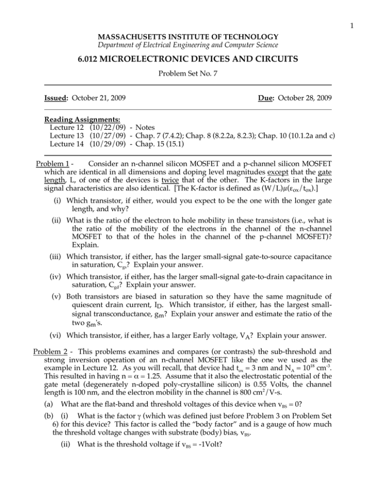
1 MASSACHUSETTS INSTITUTE OF TECHNOLOGY Department of Electrical Engineering and Computer Science 6.012 MICROELECTRONIC DEVICES AND CIRCUITS Problem Set No. 7 Issued: October 21, 2009 Due: October 28, 2009 Reading Assignments: Lecture 12 (10/22/09) - Notes Lecture 13 (10/27/09) - Chap. 7 (7.4.2); Chap. 8 (8.2.2a, 8.2.3); Chap. 10 (10.1.2a and c) Lecture 14 (10/29/09) - Chap. 15 (15.1) Problem 1 Consider an n-channel silicon MOSFET and a p-channel silicon MOSFET which are identical in all dimensions and doping level magnitudes except that the gate length, L, of one of the devices is twice that of the other. The K-factors in the large signal characteristics are also identical. [The K-factor is defined as (W/L)µ(εox/tox).] (i) Which transistor, if either, would you expect to be the one with the longer gate length, and why? (ii) What is the ratio of the electron to hole mobility in these transistors (i.e., what is the ratio of the mobility of the electrons in the channel of the n-channel MOSFET to that of the holes in the channel of the p-channel MOSFET)? Explain. (iii) Which transistor, if either, has the larger small-signal gate-to-source capacitance in saturation, Cgs? Explain your answer. (iv) Which transistor, if either, has the larger small-signal gate-to-drain capacitance in saturation, Cgd? Explain your answer. (v) Both transistors are biased in saturation so they have the same magnitude of quiescent drain current, ID. Which transistor, if either, has the largest smallsignal transconductance, gm? Explain your answer and estimate the ratio of the two gm's. (vi) Which transistor, if either, has a larger Early voltage, VA? Explain your answer. Problem 2 - This problems examines and compares (or contrasts) the sub-threshold and strong inversion operation of an n-channel MOSFET like the one we used as the example in Lecture 12. As you will recall, that device had tox = 3 nm and NA = 1018 cm-3. This resulted in having n = α = 1.25. Assume that it also the electrostatic potential of the gate metal (degenerately n-doped poly-crystalline silicon) is 0.55 Volts, the channel length is 100 nm, and the electron mobility in the channel is 800 cm2/V-s. (a) What are the flat-band and threshold voltages of this device when vBS = 0? (b) (i) What is the factor γ (which was defined just before Problem 3 on Problem Set 6) for this device? This factor is called the “body factor” and is a gauge of how much the threshold voltage changes with substrate (body) bias, vBS. (ii) What is the threshold voltage if vBS = -1Volt? 2 2 (c) How wide must the gate be to have K = 1 mA/V ? (Remember to include α.) (d) What is the drain current in saturation when this device is biased 1 Volt above threshold? (e) (i) What is the drain current in saturation when this device is biased 0.12 Volts below threshold? (ii) What is the drain current in saturation when vGS = vBS = 0? (iii) How much power is dissipated in an integrated circuit containing 106 transistors like this, each in series with a load connecting a 1.5 V power supply buss to ground [as, for example, in Figure 15.2(c) in the course text] when all of the transistors are off with vGS = 0? Problem 3 - Several three-terminal devices (e.g., vacuum tube triodes, static induction transistors, field-emitter display pixels) have characteristics like those illustrated below: i P (mA) 125 P 0V 100 -5 V 75 G -10 V 50 v GK = -15 V 25 K 0 100 iG = IG(eqVGK/kT -1) and 200 300 400 v PK (Volts) iP = G(M vPK + vGK)3/2 with G = 2 mA/V3/2, M = 0.06, and IG = 10-6 A (a) An incremental model for a device with these characteristics is illustrated below. + v gk - + gi grv pk gfv gk go v pk - Find mathematical expressions for each of the parameters in the incremental model (gi, gr, gf, and go) and evaluate these expressions at the bias point VGK = - 4 V, and VPK = 160 V. 3 (b) This device is biased using the resistor bias circuit illustrated below: + 200 V RP R G1 P G K 10 k ! 1k! - 20 V Select RG1 and RP to achieve the bias point specified in Part (a), i.e., VGK = - 4 V, and VPK = 160 V. Problem 4 (“iLab” problem) - This problem requires that you use a remote-control device measurement and characterization system called "iLab". Go to http://ilab.mit.edu, sign up for a user account if you don’t have one already (this can take a day or two, so sign up well before this problem set is due), and read the user manual provided there. After reading the manual, go to “Launch Lab” and make your measurements using the Java applet that appears. You select the device that will be under test from the "Device" menu. For this problem use one of the two devices named “3u nMOSFET” (#4 and #6). Look at the output characteristics of this device as directed below. Prepare and submit the plots requested, and give the requested parameter values. Caution: Do not let vGS exceed 3 V or vDS exceed 4 V. a) On linear scales, plot iD vs vDS for 0 ≤ vDS < 4 V, with vGS as a parameter (0 ≤ vGS ≤ 3 V) and with vBS = 0. Estimate the threshold voltage, VT, and the Early voltage, VA, for this device. b) Repeat Part (b) with vBS = - 0.5 V. c) Plot iD vs vGS, with vDS = 4 V and vBS = 0 V on a linear scale. Also plot (iD)1/2 vs vGS, and use this plot to find the threshold voltage, VT, and the K-factor of this device with vBS = 0. d) Display the plot of iD vs vGS, with vDS = 4 V and vBS = 0 V in Part (c) on a log-linear scale and use it to estimate the sub-threshold slope and the value of “n”. Also determine the factor IS,s-t in the expression for sub-threshold current (see, for example, Slide 21 in Lecture 12). 4 e) Use the techniques in Parts (c) and (d) to estimate the threshold voltage, sub threshold slope, the factor IS,s-t, and “n” when vBS = - 0.5 V. Comment on whether the changes you find from the vBS = 0 case have the right sign, and whether they seem reasonable. f) Return to your plot of iD vs vDS for 0 ≤ vDS < 4 V, with vGS as a parameter (0 ≤ vGS ≤ 3 V) and with vBS = 0 in Part (a), but only plot it for (0 ≤ vGS ≤ VT), and make it a loglinear plot, i.e., log iD vs vDS. You might even try to make the steps in vGS be nkT/q, and compare your plot to that on Slide 26 of Lecture 12. g) Optional extra fun (I am curious to see what you find): Your estimates of K, n, and ISs-t in Part (d) should all be consistent, and in fact should be related (see Slide 21 of Lecture 12). You should find: IS,s-t = Ko (kT/q)2 (n-1). What do you actually find? Note: The estimates you found in Part (e) should, of course, also be related. You may want to check that too. Additional final comments on iLab: The "auto scale" function might be useful for displaying plots. For research purposes, the system keeps a record of all logins and all scripts that each user executes. MIT OpenCourseWare http://ocw.mit.edu 6.012 Microelectronic Devices and Circuits Fall 2009 For information about citing these materials or our Terms of Use, visit: http://ocw.mit.edu/terms.
