Massachusetts Institute of Technology Department of Electrical Engineering and Computer Science 6.976
Massachusetts Institute of Technology
Department of Electrical Engineering and Computer Science
6.976
High Speed Communication Circuits and Systems
Spring 2003
Project #2: GMSK Transceivers
Passed Out: April 25, 2003 Due: May 14, 2003
Copyright c 2003 by Michael H. Perrott
Reading: Chapter 18 of Thomas H. Lee’s book. Chapter 5 of Behzad Razavi’s book.
1 Introduction
This project will explore issues associated with implementing a GMSK (Gaussian Minimum
Shift Keying) transmitter that is intended for use in GSM cell phones. This communication standard encodes information using phase modulation of a constant envelope sine wave signal. By constraining the transmitter output to have constant envelope, a nonlinear power amplifier can be used that broadcasts the signal with high efficiency (usually around 50% efficiency, as compared to about 10% efficiency encountered with linear power amps).
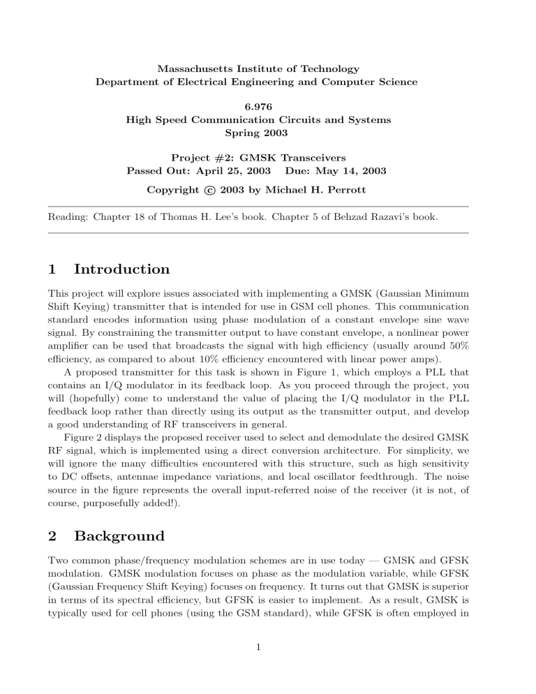
A proposed transmitter for this task is shown in Figure 1, which employs a PLL that contains an I/Q modulator in its feedback loop. As you proceed through the project, you will (hopefully) come to understand the value of placing the I/Q modulator in the PLL feedback loop rather than directly using its output as the transmitter output, and develop a good understanding of RF transceivers in general.
Figure 2 displays the proposed receiver used to select and demodulate the desired GMSK
RF signal, which is implemented using a direct conversion architecture. For simplicity, we will ignore the many difficulties encountered with this structure, such as high sensitivity to DC offsets, antennae impedance variations, and local oscillator feedthrough. The noise source in the figure represents the overall input-referred noise of the receiver (it is not, of course, purposefully added!).
2 Background
Two common phase/frequency modulation schemes are in use today — GMSK and GFSK modulation. GMSK modulation focuses on phase as the modulation variable, while GFSK
(Gaussian Frequency Shift Keying) focuses on frequency. It turns out that GMSK is superior in terms of its spectral efficiency, but GFSK is easier to implement. As a result, GMSK is typically used for cell phones (using the GSM standard), while GFSK is often employed in
1
Reference
Frequency
(100 MHz)
T
T d
T
PFD
N
I cp
Loop Filter
H(s) vin(t)
Limit
Amp
K v f o
= 30 MHz/V
= 900 MHz
90 o
Q
I out(t)
Power
Amp
0 t
Digital I/Q Generation
T t
RF Transmit
Spectrum
Trans.
Noise f
RF f cos( Φ ) D/A
Data
Generator
Gaussian
LPF f inst
K ph
1 - z
-1
Φ
Data Eye t
Peak-to-Peak
Frequency
Deviation
T d
=
1
1 MHz sin( Φ ) D/A
Includes
Zero-Order
Hold
Figure 1: A GMSK modulator implemented as an offset PLL.
Receiver
Noise
Received
Spectrum
Trans.
Noise f
RF f f
RF
N
R f
Band
Select
Filter LNA
Channel
Select
Filter cos(2 π f
RF t) sin(2 π f
RF t)
I
R
Baseband
Spectrum
0
S (
I
R
+j
Q
R
)
Modulation
Signal
Receiver
Noise
Transmitter
Noise f
Q
R
Figure 2: A direct conversion receiver for GMSK detection.
cordless phones (using the DECT standard). Note that cordless phones can get by with much lower performance (and lower cost)than their cell phone counterparts for reasons discussed in class.
Both modulation methods use a Gaussian transmit filter to smooth the data signal, as illustrated in Figure 1, in order to reduce its spectral content. This filter is implemented
2
in discrete-time with a sample period of T , and will be denoted as P [ k ]. If the input data pattern consists of modulated, unit area impulses with symbol period ( T d
) spacing between them, then the transmit filter is formulated as P [ k ] = P ( T k ) such that
P ( t ) = h
T
2
√
1
2 πσ e
− 1
2
( t
σ
)
2
∗ rect( T d
, t ) where ’*’ denotes convolution, and
(1)
σ =
.
833 T d
( BT d
)2 π
, rect( T d
, t ) =
1 /T d
0 ,
, − T d
2
≤ t ≤ elsewhere .
T d
2
In the case where the data is “square-wave” in nature, as shown in Figure 1, then one simply removes the rect function (and the associated convolution operation) in the above formulation (note that you will need to appropriately scale the response, as discussed later).
In either case, P [ k ] is parameterized by two characteristics:
•
BT d
: ratio of bandwidth of P ( e j
2
πf T
) to data rate
• h : modulation index, defined as: h = peak-to-peak frequency deviation bit rate
For the popular standards of GSM and DECT, we are required to have:
•
GSM: BT d
= 0 .
3, h = 0 .
5
•
DECT: BT d
= 0 .
5, h = 0 .
5
± .
05
Therefore, both specify the modulation index to be h=0.5 — for GSM, this value must be exactly maintained, while for DECT it can vary
±
10% about that nominal value. However,
GSM requires the BT d product to be much lower, which implies a much better spectral efficiency (i.e., required bandwidth for a given data rate).
The impact of the different BT d products for GSM and DECT can be viewed in the time or frequency domains. Here we focus on the time domain, and use eye diagrams to convey the key issues. Figure 3 illustrates ideal eye diagrams for the instantaneous frequency and phase signals corresponding to a GSM transmitter with BT d
= 0 .
3. In this case, we are interested only in phase (since GMSK is used), and therefore the I/Q diagrams are of primary interest. Note that the eye for instantaneous frequency is relatively poor compared to its I/Q counterpart — extraction of the modulation information based on frequency would therefore yield rather poor performance (which is further exacerbated by issues related to synchronous vs asynchronous demodulation, a topic we will not touch on here).
Figure 3 illustrates ideal eye diagrams corresponding to a DECT transmitter implementing GFSK with BT d
= 0 .
5. For GFSK, we are concerned with the instantaneous frequency rather than the I/Q components. Note that the eyes for instantaneous frequency (as well as its I/Q counterpart) are quite open compared to the GSM modulator. We therefore see that high vales of BT d lower the level of intersymbol interference at the cost of poorer spectral
3
6
4
2
8 x 10
5
0
−2
−4
−6
−8
0 0.2
Simulated Eye Diagram of Instantaneous Frequency
0
−0.5
−1
1
0.5
−0.5
−1
1
0.5
0
2
Simulated Eye Diagram of I Component
4 6 8
Time (Seconds)
10
Simulated Eye Diagram of Q Component
12 14 16 x 10
−7
0.4
0.6
0.8
time (Seconds)
1
(a)
1.2
1.4
1.6
x 10
−6
2 4 6 8
Time (Seconds)
10
(b)
12 14 16 x 10
−7
Figure 3: Eye diagrams correponding to GMSK modulation with BT d of instantaneous frequency, (b) eye diagrams of I and Q components
= 0 .
3: (a) eye diagram efficiency. A final issue is that one would observe the I/Q eye diagrams undergo catastrophic degradation should the value of h vary even slightly from 0.5, while the instantaneous frequency eye diagram would simply change in amplitude while still remaining wide open. Since frequency is the signal of interest in this case, GFSK systems allow such sloppiness in the control of h , whereas GMSK system are intolerant of it.
4
2
0
8 x 10
5
6
−2
−4
−6
−8
0 0.2
Simulated Eye Diagram of Instantaneous Frequency
0
−0.5
−1
1
0.5
1
−0.5
−1
0.5
0
2
Simulated Eye Diagram of I Component
4 6 8
Time (Seconds)
10
Simulated Eye Diagram of Q Component
12 14 16 x 10
−7
0.4
0.6
0.8
time (Seconds)
1
(a)
1.2
1.4
1.6
x 10
−6
2 4 6 8
Time (Seconds)
10
(b)
12 14 16 x 10
−7
Figure 4: Eye diagrams correponding to GFSK modulation with BT d of instantaneous frequency, (b) eye diagrams of I and Q components
= 0 .
5: (a) eye diagram
The transmitter structure shown in Figure 1 achieves accurate phase modulation, and can be used for either GMSK or GFSK systems. However, the ability of GFSK systems to endure sloppiness in their modulation index, h , allows for simpler transmitter structures. In fact, it is not uncommon for GFSK modulators to be implemented by directly modulating
4
a VCO.
While the GMSK receiver shown in Figure 2 appears to be quite simple, it is quite challenging to implement in practice. In comparison, Figure 5 illustrates a GFSK receiver based on a phase-locked loop architecture. Here the receive VCO tracks the phase of the input signal after it has been filtered and passed into a limit amplifier, and the resulting instantaneous frequency signal is obtained by observing the input voltage to the VCO. Though this design may appear to be more complex than its GMSK counterpart, it is easier to implement in practice.
N
R
Channel
Filter
Limiter
Channel
Filter 2
F out
(t)
Demodulated
Data Signal
Phase
Det.
Loop
Filter sin(2
π( f if t+F out
(t))) sin(2
π( f c
-f if
)t)
Figure 5: A GFSK receiver based on a PLL frequency descriminator.
3 Tasks
We now turn our attention entirely to GMSK, and focus first on the design of the transmitter structure shown in Figure 1. We will do so in steps, examining first the I/Q generation, then the PLL design, and then simulation of the overall system. We will then turn our attention on the receiver, particularly with respect to its simulation. In all cases, you should assume the following:
•
Modulation data rate (1 /T d
) = 1 Mbit/s
•
Reference clock rate (1 /T ) = 100 MHz
•
Center frequency of RF output spectrum f
RF
= 900 MHz
•
Tristate PFD is used for the PLL,
•
VCO has no parastic poles, so that its small signal voltage-to-phase model is simply
2 πK v
/s ,
•
VCO noise (output referred) has a slope of -20 dB/dec over the frequency range of interest, with a value of -140 dBc/Hz at 10 MHz offset
•
Simulation sample rate = 9 GHz.
Note that, in practice, the GSM standard actually has a data rate of roughly 270 kbit/s — we are striving to increase it by a factor of 4.
5
1. In this task we will implement the I/Q generator block shown in Figure 6 using the
CppSim simulator. The following subsections will guide you through this process.
T Reference
Frequency
(100 MHz)
T d
T
Digital I/Q Generation
T t t cos( Φ ) D/A
Data
Generator
Gaussian
LPF f inst
K ph
1 - z
-1
Φ sin( Φ ) D/A
Data Eye t
Peak-to-Peak
Frequency
Deviation
Includes
Zero-Order
Hold
T d
=
1
1 MHz
Figure 6: digital I/Q generator.
(a) Implement the data generator and Gaussian transmit filter in CppSim, and plot the resulting eye diagrams produced by a data sequence consisting of 30 symbols.
i. Use Matlab to compute the filter tap coefficients of the Gaussian transmit filter over 5 symbol periods. Assume the sampling period of the tap coefficients corresponds to that of the reference frequency, and that the input data sequence will be “square” wave in nature (i.e., don’t convolve with the rectangle function, but you do need to figure out the appropriate scaling factor based on the reference frequency and symbol rate value. To do so, recall that the peak-to-peak frequency deviation that occurs after passing the prbs data sequence into the Gaussian filter must match that specified by h and T d
. Assume that the prbs data sequence alternates between 1 and -1 and is sampled according to the reference frequency). Plot the filter impulse response over 5 symbol periods using the stem command in Matlab.
ii. Create the prbs data source module in CppSim using the Rand class (“bernoulli” behavior). To do so, you will need to clock the Rand object according to an input clock (which will be fed by the reference frequency) such that it updates its output value at the correct data rate. Note: see the next part to see how to “clock” objects. Plot the output of the module and its eye diagram over 30 symbols (you can use the vco module to create the 100 MHz reference clock).
Note that the output should alternate between 1 and -1.
iii. Create the Gaussian transmit filter module in CppSim. To do so, save the
6
filter coefficients computed in Matlab to a file (make sure that you save in
ASCII format, and that the coefficients are in “vertical” format in the file
(i.e., one coefficient per line)). To give you an idea of how to realize the module code in modules.par, consider the following example: module: sqrt raised cos filter parameters: inputs: double in , double clk outputs: double out classes: Filter filt
(
"1"
,
"1"
),
List list1
(),
EdgeDetect clkedge
() static variables: init: list1
.
load
(
"rcosflt.dat" filt
.
set
( list1
,
"1"
);
); code: if
( clkedge
.
inp
( clk
))
{ filt
.
inp
( in
); out = filt .
out ;
}
10
Plot the output of the cascaded data source and Guassian filter, and its eye diagram, over 30 symbols. Label the peak-to-peak frequency deviation and symbol period in the eye diagram.
(b) Implement the remaining I/Q generator blocks, simulate its output over 30 symbols, and then create an overall symbol for it.
i. Compute the value of K ph in the frequency-to-phase converter block. To do so, assume that the sample period corresponds to the reference frequency,
1 /T , and recall that z corresponds to e jwT by the equation
Φ( t ) = 2 π and phase is related to frequency
0 t f inst
( τ ) dτ ii. Implement the frequency-to-phase converter block and the cosine and sine converter functions in CppSim (combine the cosine and sine converters in one module). Again assume that all blocks are clocked by the reference frequency, and be sure to use the Filter class to implement the accumulator function for the frequency-to-phase converter block. Plot the I and Q signals, along with their eye diagrams, over 30 symbols.
iii. You have now completed the digital portion of the I/Q generator, so place each of your blocks (though not the reference frequency source) into a schematic called dig iq generator that has a clock input and I/Q outputs. For the exercises that follow, note that the D/A converters do not need to be added in
CppSim since our digital blocks are implemented in analog fashion, and the zero-order hold function is implemented intrinsicly.
(c) Now put RC lowpass filters at the outputs of the I and Q outputs of the I/Q
Generator (note that these will *not* be clocked by the reference). Set the cutoff
7
frequency of the filters first to 500 kHz and then to 10 MHz, and plot the resulting
I/Q diagrams at the filter outputs for each case. Why does the 500 kHz version look distorted? Assume that the cutoff frequency will be 10 MHz for the following task sections.
2. We will now focus on modeling and design of the PLL portion of the transmitter shown in Figure 7. You will need to use the PLL Design Assistant program, as used in HW6, to complete the design exercises.
Reference
Frequency
(100 MHz)
T
PFD I cp
N
Loop Filter
H(s) vin(t)
Limit
Amp
K v f o
= 30 MHz/V
= 900 MHz
Q
90 o
I out(t)
RF Transmit
Spectrum
Power
Amp
Trans.
Noise
0 sin( Φ ) cos( Φ ) f
RF f
Figure 7: PLL portion of the GMSK transmitter.
(a) Model the relationship between the phase signal, Φ( t ), the phase of the VCO output, Φ out
( t ), and the output phase of the I/Q modulator block, Φ out2
( t ), as labeled in Figure 8. Do this in two steps. First, express the VCO output as a sine wave, and compute the resulting I/Q modulator output in terms of a sine wave.
Based on this result, draw a block diagram of the relationship between the phase signals.
out(t)
Q
I
90 o out2(t) sin(
Φ
) cos(
Φ
)
Figure 8: Analog I/Q modulator block.
8
(b) Based on your block diagram in the previous part, draw the linearized, frequencydomain block diagram model of the PLL system shown in Figure 7. Provide an expression for the open loop gain function, A ( s ). For parts to follow, we will define the closed loop function G ( f ) to be
G ( f ) =
A ( f )
1 + A ( f )
(c) Compute the transfer function from the phase signal, Φ( t ), to the VCO output phase, Φ out
( t ) in terms of G ( f ). We will refer to this function as B ( s ) in the parts to follow.
i. Is B ( s ) lowpass, bandpass, or highpass?
ii. If we instead look at the sine wave signals associated with out
( t ), etc., rather than their respective phases, is the filtering action performed by the PLL lowpass, bandpass, or highpass? What are the advantages of using the PLL to implement the filter over simply using a passive filter?
(d) Given your answer in the previous part, do you see any advantage of incorporating the I/Q modulator in the feedback loop of the PLL rather than simply using the
I/Q modulator as the transmitter (i.e., with a PLL only being used to provide a static local oscillator signal)? Consider noise, as well as mixer nonidealities such as LO feedthrough, in formulating your answer.
(e) Design the PLL such that the B ( s ) transfer function corresponds to a second order Butterworth filter response with a bandwidth of 2 MHz. Assume a type I implementation for the PLL, a charge pump current of 100 µ A, and a K v value of 30 MHz/V. In particular, compute the divide value, N , the loop filter transfer function, H ( s ), and the PFD gain factor, α .
(f) Repeat the previous design exercise for the case where B ( s ) corresponds to a second order Butterworth filter response with a bandwidth of 4 MHz that is cascaded with two real-valued parasitic poles placed at 12 and 17 MHz.
(g) Calculate the input-referred voltage noise to the VCO that yields to its phase noise conforming to the specifications given at the beginning of the Tasks section
(i.e., -140 dBc/Hz at 10 MHz offset).
3. We will now implement the PLL circuit in CppSim and combine it with the I/Q generator module. This task should be fairly straightforward given your experience in
Homework 6, but there are a few hurdles to overcome that we will step you through.
(a) Implement the I/Q modulator shown in Figure 8 in CppSim by creating ideal mixer blocks and the limit amp module, and then combining those modules with the adder module in a schematic/symbol called phase shifter. Assume that the
I/Q modulator has two inputs corresonding to the VCO output and its quadrature component (i.e., don’t implement the 90 degree phase shifter).
9
i. When creating the limit amp module, you must understand that the output of the I/Q modulator is essentially a sine wave, but that the input to the divider assumes a square-wave with interpolated edges as discussed in the paper located at /mit/6.976/CppSim/Doc/paper.pdf. The following is suggested code to implement the limit amp — explain what the code is doing.
module
: phase shifter limit amp parameters : inputs
: double in outputs
: double out classes
: static variables : double prev in , int state init
: state
= − 2; prev in = 0.0; out = − 1.0; code
: if
( state
== − 2 && in
> = 0.0) / ∗ positive transition ∗ /
{ out
= ( in
+ prev in
) / ( in
− prev in
); state
= 1;
} else if ( state == 1)
{ out
= 1.0; state = 2;
} else if
( state
== 2 && in
< 0.0) / ∗ negative transition ∗ /
{ out = − ( in + prev in ) / ( in − prev in ); state
= − 1;
} else if
( state
== − 1)
{ out
= − 1.0; state
= − 2;
} prev in = in ;
10
20
30
(b) Implement the VCO by modifying the vco module already included in the Cpp-
Modules library such that it now has quadrature sine wave outputs (i.e., cosine and sine functions of the VCO phase). These outputs will connect up to the inputs of the I/Q modulator just implemented.
(c) Now implement the overall PLL in CppSim, and choose the various parameters so that the dynamics conform to those calculated in Task 2, part (e) (do not include noise sources). Include the I/Q generator from Task 1, and name the overall schematic pll transmitter. Simulate the overall system over 30 symbols and plot the voltage at the input to the VCO and its eye diagram (you may want to cut out the initial transient when plotting the eye diagram). Relate this signal to the
10
instantaneous frequency waveform that you should expect to see. Troubleshoot your simulation if it does not agree with what you expect to see.
(d) In Cadence, copy pll transmitter to a new schematic called pll transmitter2. Adjust the parameters in pll transmitter2 so that its dynamics conform to those calculated in Task 2, part (f). As in the previous part, simulate the overall system over 30 symbols and plot the voltage at the input to the VCO and its eye diagram. Do you see any change in performance in the eye diagram (i.e., is it better or worse?)? Why did it change?
(e) Plot the output spectrum of the pll transmitter module using the comp psd Matlab script as done in Homework 6 (note that you may need to adjust some things in the script to match the given system). You will want to dramatically increase the number of symbols to achieve a nice plot. Also, you will need to take advantage of CppSim’s ability to decimate signals before they are saved in the output file in order to simulate over a long enough time span — see the description of the “output:” command on pages 32-33 of the CppSim manual.
(f) Add VCO noise according to your calculations in Task 2, part (g), and then plot the resulting output spectrum as done in the previous part. Compare the spectrum before and after adding VCO noise — do the results make sense? Note that, in practice, there would also be detector noise in the PLL and quantization noise from the D/A. We have ignored such sources in the current assignment for the sake of simplicity, but they would be fairly straightforward to add to the simulation.
4. We now examine the receiver, and will implement a simplified version of it shown in
Figure 9 in the CppSim framework.
Receiver
Noise
Received
Spectrum
Trans.
Noise pll_transmitter f
RF output f f
RF
N
R f cos(2
Channel
Select
Filter
π sin(2 π f f
RF
RF t) t)
I
R
Baseband
Spectrum
SNR
0
S (
I
R
+j
Q
R
)
Modulation
Signal
Receiver
Noise
Transmitter
Noise f
Q
R
Figure 9: Simplified GMSK receiver to be implemented in CppSim.
(a) Implement the receiver shown in Figure 9. Assume that the noise source has zero variance (for now), and that each channel select filter is simply a pair of cascaded first order filters with a cutoff frequency of 5 MHz (DC gain of 1). Create an overall Cadence symbol for the receiver called simple iq receiver that has 3 inputs
11
(to receive transmitter output and the quadrature sine waves at frequency f RF ) and two outputs (the baseband I/Q signals).
(b) Now create a schematic that combines the pll transmitter and simple iq receiver blocks and also supplies the required LO frequency to the receiver. We will assume an ideal channel, so simply connect the transmitter output to the receiver input.
To create the quadrature LO signal, use the VCO block you created in Task 3 that produces quadrature sine waves. Simulate the system over 30 symbol periods and plot the resulting I/Q signals at the receiver output along with their eye diagrams.
Note that you may need to adjust the phase of the LO signal to the receiver in order to get your eye diagrams to look right — explain why that is the case (hint: think about the I/Q signals in terms of constellation points).
(c) Compute the value of the receiver noise variance that will yield an SNR of 10 dB at the I/Q outputs of the receiver (assume that the noise is added as shown in
Figure 9). Here we define SNR as the ratio of the spectral density of the received signal to the spectral density of the noise at low frequencies, as shown in the figure. Simulate the overall system with the included noise and plot the resulting
I/Q eye diagrams.
(d) Given the added noise of the receiver, what are the tradeoffs between having a large versus small bandwidth for the receiver channel select filter?
5. We have so far assumed that we only want to modulate in a channel that is centered at
900 MHz. Suppose that you wanted to use the same RF transmit architecture (with a constant reference freqeuncy of 100 MHz), but wanted to be able to change the center frequency in 1 MHz steps. Explain how you would modify the transmitter architecture to accomplish this task, and prove it by simulating your modified structure in CppSim with f
RF
= 901 MHz.
12
