MASSACHUSETTS INSTITUTE OF TECHNOLOGY
advertisement
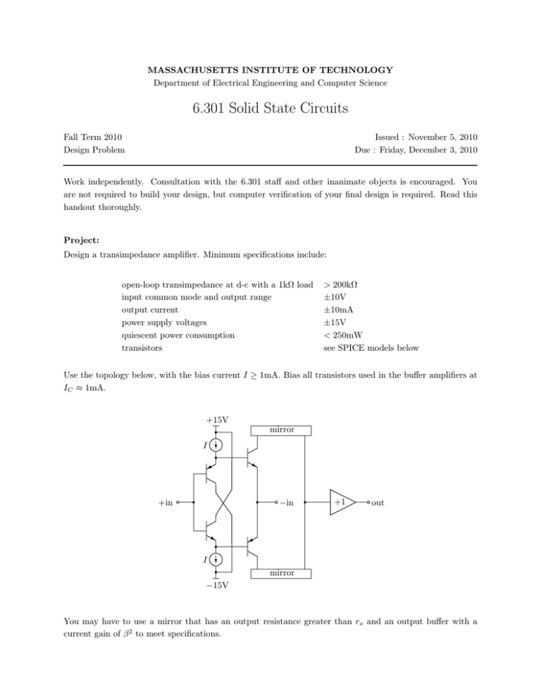
MASSACHUSETTS INSTITUTE OF TECHNOLOGY Department of Electrical Engineering and Computer Science 6.301 Solid State Circuits Fall Term 2010 Design Problem Issued : November 5, 2010 Due : Friday, December 3, 2010 Work independently. Consultation with the 6.301 staff and other inanimate objects is encouraged. You are not required to build your design, but computer verification of your final design is required. Read this handout thoroughly. Project: Design a transimpedance amplifier. Minimum specifications include: open-loop transimpedance at d-c with a 1kΩ load input common mode and output range output current power supply voltages quiescent power consumption transistors > 200kΩ ±10V ±10mA ±15V < 250mW see SPICE models below Use the topology below, with the bias current I ≥ 1mA. Bias all transistors used in the buffer amplifiers at IC ≈ 1mA. +15V mirror I +in −in +1 out I mirror −15V You may have to use a mirror that has an output resistance greater than ro and an output buffer with a current gain of β 2 to meet specifications. 1 Assignment: There are two options for this assignment: you may either simulate your design in SPICE, or build it. Note that construction is not required for this project, and that either option will be graded with equal weight. 1.1 OPTION 1: Simulation For this option, use the SPICE models below. You may use ideal current sources for biasing. Work out a preliminary design based upon typical numbers from the transistor models. Analyze the circuit by hand, making reasonable approximations. In your report, convince us that you understand this topology. Show that your design meets the specifications listed above. Then connect your design as shown below. R − vo vi + 1kΩ The transfer function vvoi (jω) has an angle of −180◦ at low frequencies, and the angle becomes more negative as frequency increases. Determine a value for R that results in an angle of −225◦ when the | vvoi (jω)| = 1 (that is, results in a phase margin of 45◦ ). Then connect your amplifier as shown to get a nominal closed loop gain of 11. + vi vo − R R/10 What is the bandwidth of your amplifier in this connection? What is the actual closed-loop gain at low frequencies? Your report should be short and informal. Include appropriate plots to support that your design meets all specifications. Transistor models: * Q[name] Nc Nb Ne [model name] .model npn1 npn is=15fA bf=200 vaf=50 cje=10p tf=750p cjc=1p .model pnp1 pnp is=15fA bf=50 vaf=25 cje=10p tf=750p cjc=1p 1.2 OPTION 2: Construction For this option, you are not required to simulate your design. MIT OpenCourseWare http://ocw.mit.edu 6.301 Solid-State Circuits Fall 2010 For information about citing these materials or our Terms of Use, visit: http://ocw.mit.edu/terms.
