Recitation 21: Intrinsic Frequency Response of CS & CE Amplifier
advertisement
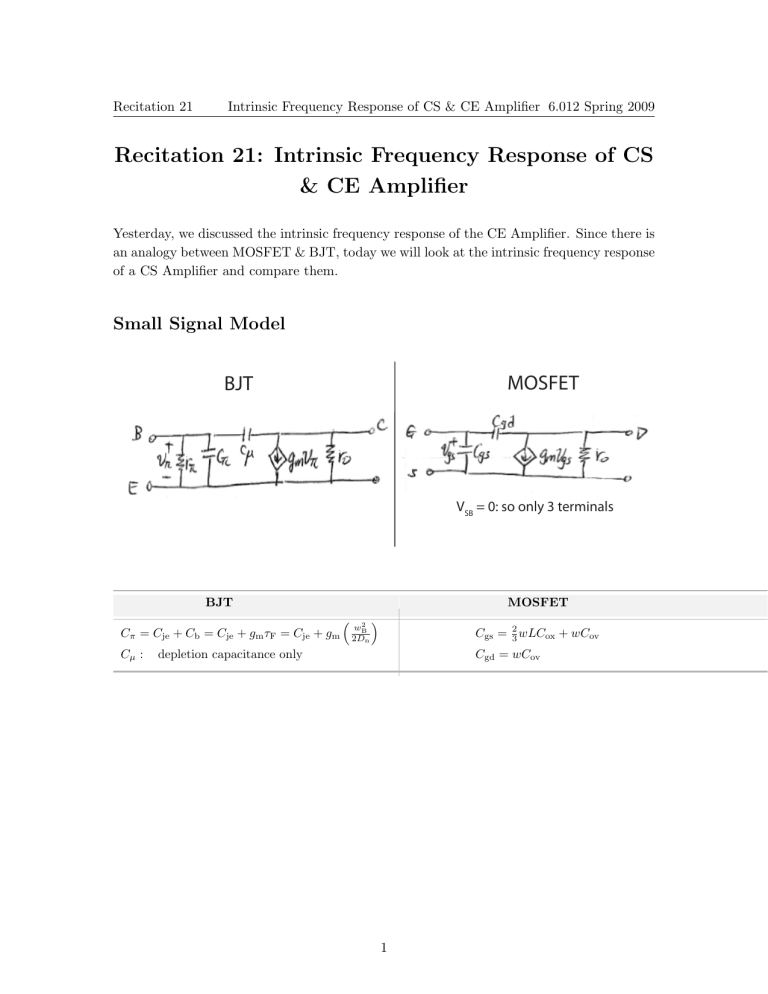
Recitation 21 Intrinsic Frequency Response of CS & CE Amplifier 6.012 Spring 2009 Recitation 21: Intrinsic Frequency Response of CS & CE Amplifier Yesterday, we discussed the intrinsic frequency response of the CE Amplifier. Since there is an analogy between MOSFET & BJT, today we will look at the intrinsic frequency response of a CS Amplifier and compare them. Small Signal Model MOSFET BJT VSB = 0: so only 3 terminals BJT Cπ = Cje + Cb = Cje + gm τF = Cje + gm Cμ : MOSFET 2 wB 2D n Cgs = 23 wLCox + wCov Cgd = wCov depletion capacitance only 1 Recitation 21 Intrinsic Frequency Response of CS & CE Amplifier 6.012 Spring 2009 Intrinsic Frequency Response: Rs → ∞ RL = 0 BJT Node 1: iin = vπ γπ MOSFET Node 1: iin = jwCgs · Vgs + jwCgd Vgs + jwCπ · vπ + jwCμ vπ Node 2: iout = gm vπ − jwCμ vπ jwCμ g γ 1 − m π gm iout = 1 + jwγ (C iin π π +C μ ) jwCμ βo 1 − gm = 1 + jwγπ (Cπ + Cμ ) Node 2: iout = gm vπ − jw iout gm − jwCgd = jw(Cgs + Cgd ) iin 2 Recitation 21 Intrinsic Frequency Response of CS & CE Amplifier 6.012 Spring 2009 Unit Gain Frequency, fT BJT MOSFET 1 1 gm wT = 2π 2π Cμ + Cπ Frequency at which the current gain is reduced to 1(0 dB) This is obtained by: jwCμ i βo 1 − g out m = =1 iin 1 + jwγπ (Cμ + Cπ ) fT = gm ignoring the zero on top, ∵ wT Cμ βo =1 1 + jwγπ (Cμ + Cπ ) ∵ wT γπ (Cμ1+Cπ ) ∴ wT γπ (Cμ + Cπ ) 1 βo gm = 1 =⇒ wT = jwγπ (Cμ + Cπ ) Cμ + Cπ fT = 1 gm 2π Cgs + Cgd (this can be derived similar to the BJT case) fT = Physical interpretation: gm 2π(Cgs + Cgd ) 1 gm 1 w/Lμn Cox (VGS − 1) 2π Cgs 2π 2/3wLCox 1 3 μn (VGS − VT ) 3 μn VD,SAT 1 = 2 2π 2 2 L2 2π L μn VDSAT ∼ velocity of carrier L fT = μn VDSAT /L ∼ 1/τT = τT = L/ velocity L τT is transit time from source to drain 1 Ic /Vth Ic + Cje + Cμ (∵ gm = ) Vth 2π Ic /Vth · τF fT is independent of V . For high frequency performance, NMOS > PMOS. Scale L as short as possible 3 Recitation 21 Intrinsic Frequency Response of CS & CE Amplifier 6.012 Spring 2009 At low Ic , fT is dominated by depletion capacitances at Base-emitter and base collector junctions (Cje and Cμ ). As Ic ↑, diffusion capacitance gm τF ↑, and becomes dominant. Fundamental limit for frequency response 2 wB τF = 2Dn,p To increase fT - high Ic = diffusion cap. limited =⇒ shrink base width. - low Ic = depletion cap. limited =⇒ shrink device area 4 Another note for MOSFET: the current gain → ∞ at w = 0. This is because of gate oxide, DC input current = 0. MOSFET not used as current amplifier at low frequency (input resistance too high) MIT OpenCourseWare http://ocw.mit.edu 6.012 Microelectronic Devices and Circuits Spring 2009 For information about citing these materials or our Terms of Use, visit: http://ocw.mit.edu/terms.
