Systems Single Photon Avalanche Diodes Differential APS Introduction
advertisement

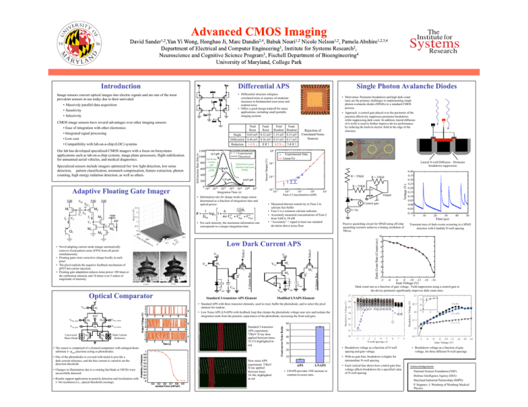
The Institute for Systems Research Differential APS • Massively parallel data acquisition • Sensitivity • Selectivity CMOS image sensors have several advantages over other imaging sensors: • Ease of integration with other electronics • Integrated signal processing • Low cost • Compatibility with lab-on-a-chip (LOC) systems Adaptive Floating Gate Imager Single Fund. Reset Total Readout • Motivation: Perimeter breakdown and high dark count rates are the primary challenges to implementing single photon avalanche diodes (SPADs) in a standard CMOS process. Fund. Readout Rejection of Correlated Noise Sources 0.65 mV 0.12 mV 1.15 mV 0.13 mV Differential 0.46 mV 0.36 mV 0.13 mV 0.17 mV 1.4 X ↓ Reduction 1200 1000 800 600 Falloff due to pixel saturation and scene change 4.38 pW 400 1.27 pW 200 0 10-5 10-4 10-3 10-2 0.127 pW 10-1 10-0 9.2 X ↓ 100 Experimental Theoretical 12.7 pW Falloff due to noise and limited use of DR 3X↑ 101 Integration Time (s) • Information rate for charge mode image sensor determined as a function of integration time and optical power: • For each intensity, the maximum information rate corresponds to a unique integration time Sensor Output (V) Specialized sensors include imagers optimized for: low light detection, low noise detection, pattern classification, mismatch compensation, feature extraction, photon counting, high energy radiation detection, as well as others. Total Reset Information Rate (bits/s) Our lab has developed specialized CMOS imagers with a focus on biosystems applications such as lab-on-a-chip systems, image plane processors, flight stabilization for unmanned aerial vehicles, and medical diagnostics. Single Photon Avalanche Diodes • Differential structure mitigates correlated noise at expense of moderate increases in fundamental reset noise and readout noise • Offers a good design tradeoff for many applications, including small portable imaging systems 1.4 X ↑ • Approach: a control gate placed over the perimeter of the junction effectively suppresses perimeter breakdown while suppressing dark count. In addition, lateral diffusion of n-wells is used to further improve device performance by reducing the built-in electric field at the edge of the structure. 90 µm Experimental Data Linear Fit Lateral N-well Diffusion – Perimeter breakdown suppression 10-1 R = 35KΩ 10-2 R = 35KΩ Voltage (V) Introduction Image sensors convert optical images into electric signals and are one of the most prevalent sensors in use today due to their unrivaled R = 35KΩ 10-3 -3 10 10-2 10-1 100 Fura-2 Concentration (mM) 101 • Measured detector sensitivity to Fura-2 in calcium free buffer • Fura-2 is a common calcium indicator • Accurately measured concentrations of Fura-2 from 5uM to 39 nM • “Accurately” = signal at least one standard deviation above noise floor Output Control gate V=Va 0.40 0.35 0.30 0.25 0.20 0.15 0.10 0.05 0.00 -0.05 -0.10 0 Passive quenching circuit for SPAD using off-chip quenching resistors achieves a timing resolution of 500 ns. 10 20 30 Time (µs) 40 50 Transient trace of dark events occurring in a SPAD structure with 6 lambda N-well spacing Optical Comparator Vout_plus Uncovered Photo Diode Standard 3-transistor APS Element Select M2 Vpd Cpd M3 M4 Cint Column Bus Select Cpd Cint Column Bus M2 7 6 5 4 3 2 -2 -4 -6 -8 -10 -12 Gate Voltage (V) -14 -16 Dark count rate as a function of gate voltage. Field suppression using a control gate at the device perimeter significantly improves dark count rates. Modified LNAPS Element Vbias_minus Vout_minus M5 M1 M1 Vrst 8 • Low Noise APS (LNAPS) with feedback loop that clamps the photodiode voltage near zero and isolates the integration node from the parasitic capacitance of the photodiode, increasing the front-end gain. M4 M3 M1 9 • Standard APS with three transistor elements, used to reset, buffer the photodiode, and to select the pixel element for readout. M6 RST Vbias_plus Vrst Vdd M2 Dark Current Reference • The sensor is comprised of a clocked comparator with enlarged drainsubstrate n+-psub junctions acting as photodiodes. • One of the photodiodes is covered with metal to provide a dark current reference, and the bias current is varied to set the detection threshold. • Changes in illumination due to a rotating fan blade at 100 Hz were successfully detected. • Results support application to particle detection and localization with 1- bit resolution (i.e., optical threshold crossing). 60 Standard 3-transistor APS experiment: 75KeV X-ray dose applied between times 35-37s highlighted in red Now-noise APS experiment: 75KeV X-ray applied between times 18-30s, highlighted in red Contrast-to-Noise Ratio Vbias Vdd M3 • Novel adapting current mode imager automatically removes fixed pattern noise (FPN) from all pixels simultaneously. • Floating gates store corrective charge locally in each pixel. • The pixel exploits the negative feedback mechanism of pFET hot-carrier injection. • Floating gate adaptation reduces noise power 100 times at the calibration intensity and 10 times over 5 orders of magnitude of intensity. Dark Count Rate (Counts/sec) 10 Low Dark Current APS 50 40 30 • Breakdown voltage as a function of N-well spacing and gate voltage. 20 10 • Breakdown voltage as a function of gate voltage, for three different N-well spacings. • With no gate bias, breakdown is higher for intermediate N-well spacing. APS LNAPS • LNAPS provides 10X increase in contrast-to-noise ratio. • Each vertical line shows how control gate bias voltage affects breakdown for a specified value of N-well spacing. Acknowledgements National Science Foundation (NSF) Defense Intelligence Agency (DIA) Maryland Industrial Partnerships (MIPS) P. Stepanov, I. Weinberg of Weinberg Medical Physics


