Research Journal of Applied Sciences, Engineering and Technology 4(5): 486-490,... ISSN: 2040-7467 © Maxwell Scientific Organization, 2012
advertisement
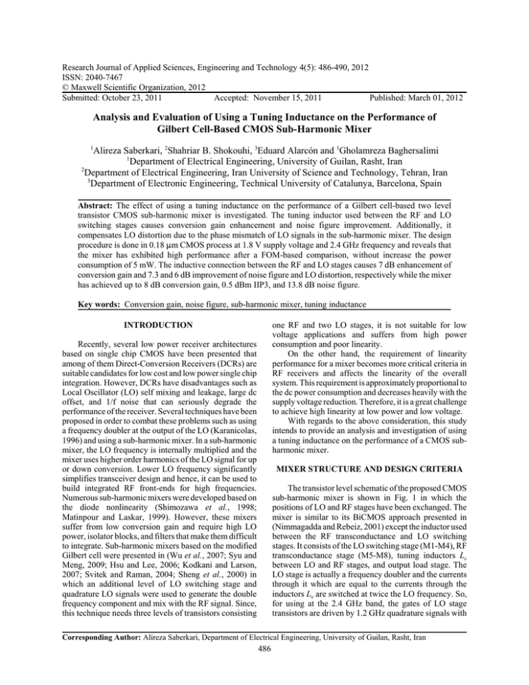
Research Journal of Applied Sciences, Engineering and Technology 4(5): 486-490, 2012 ISSN: 2040-7467 © Maxwell Scientific Organization, 2012 Submitted: October 23, 2011 Accepted: November 15, 2011 Published: March 01, 2012 Analysis and Evaluation of Using a Tuning Inductance on the Performance of Gilbert Cell-Based CMOS Sub-Harmonic Mixer 1 Alireza Saberkari, 2Shahriar B. Shokouhi, 3Eduard Alarcón and 1Gholamreza Baghersalimi 1 Department of Electrical Engineering, University of Guilan, Rasht, Iran 2 Department of Electrical Engineering, Iran University of Science and Technology, Tehran, Iran 3 Department of Electronic Engineering, Technical University of Catalunya, Barcelona, Spain Abstract: The effect of using a tuning inductance on the performance of a Gilbert cell-based two level transistor CMOS sub-harmonic mixer is investigated. The tuning inductor used between the RF and LO switching stages causes conversion gain enhancement and noise figure improvement. Additionally, it compensates LO distortion due to the phase mismatch of LO signals in the sub-harmonic mixer. The design procedure is done in 0.18 :m CMOS process at 1.8 V supply voltage and 2.4 GHz frequency and reveals that the mixer has exhibited high performance after a FOM-based comparison, without increase the power consumption of 5 mW. The inductive connection between the RF and LO stages causes 7 dB enhancement of conversion gain and 7.3 and 6 dB improvement of noise figure and LO distortion, respectively while the mixer has achieved up to 8 dB conversion gain, 0.5 dBm IIP3, and 13.8 dB noise figure. Key words: Conversion gain, noise figure, sub-harmonic mixer, tuning inductance INTRODUCTION one RF and two LO stages, it is not suitable for low voltage applications and suffers from high power consumption and poor linearity. On the other hand, the requirement of linearity performance for a mixer becomes more critical criteria in RF receivers and affects the linearity of the overall system. This requirement is approximately proportional to the dc power consumption and decreases heavily with the supply voltage reduction. Therefore, it is a great challenge to achieve high linearity at low power and low voltage. With regards to the above consideration, this study intends to provide an analysis and investigation of using a tuning inductance on the performance of a CMOS subharmonic mixer. Recently, several low power receiver architectures based on single chip CMOS have been presented that among of them Direct-Conversion Receivers (DCRs) are suitable candidates for low cost and low power single chip integration. However, DCRs have disadvantages such as Local Oscillator (LO) self mixing and leakage, large dc offset, and 1/f noise that can seriously degrade the performance of the receiver. Several techniques have been proposed in order to combat these problems such as using a frequency doubler at the output of the LO (Karanicolas, 1996) and using a sub-harmonic mixer. In a sub-harmonic mixer, the LO frequency is internally multiplied and the mixer uses higher order harmonics of the LO signal for up or down conversion. Lower LO frequency significantly simplifies transceiver design and hence, it can be used to build integrated RF front-ends for high frequencies. Numerous sub-harmonic mixers were developed based on the diode nonlinearity (Shimozawa et al., 1998; Matinpour and Laskar, 1999). However, these mixers suffer from low conversion gain and require high LO power, isolator blocks, and filters that make them difficult to integrate. Sub-harmonic mixers based on the modified Gilbert cell were presented in (Wu et al., 2007; Syu and Meng, 2009; Hsu and Lee, 2006; Kodkani and Larson, 2007; Svitek and Raman, 2004; Sheng et al., 2000) in which an additional level of LO switching stage and quadrature LO signals were used to generate the double frequency component and mix with the RF signal. Since, this technique needs three levels of transistors consisting MIXER STRUCTURE AND DESIGN CRITERIA The transistor level schematic of the proposed CMOS sub-harmonic mixer is shown in Fig. 1 in which the positions of LO and RF stages have been exchanged. The mixer is similar to its BiCMOS approach presented in (Nimmagadda and Rebeiz, 2001) except the inductor used between the RF transconductance and LO switching stages. It consists of the LO switching stage (M1-M4), RF transconductance stage (M5-M8), tuning inductors Le between LO and RF stages, and output load stage. The LO stage is actually a frequency doubler and the currents through it which are equal to the currents through the inductors Le are switched at twice the LO frequency. So, for using at the 2.4 GHz band, the gates of LO stage transistors are driven by 1.2 GHz quadrature signals with Corresponding Author: Alireza Saberkari, Department of Electrical Engineering, University of Guilan, Rasht, Iran 486 Res. J. Appl. Sci. Eng. Technol., 4(5): 486-490, 2012 LO DISTORTION IMPROVEMENT Another benefit of using the tuning inductor is that with presence of Le , LO distortion due to the phase mismatch of LO signals is improved. We assume that the LO signals driving the gates of LO stage transistors are as below: a cos(ω LO t ) 2 a π v LO,90 = cos(ω LO t + + θ 2 ) 2 2 a v LO,180 = cos(ω LO t + π + θ1 ) 2 3π a v LO,270 = cos(ω LO t + + θ 2 + θ1 ) 2 2 v LO,0 = (1) Fig. 1: Schematic of the proposed mixer where, 21 and 22 are phase mismatch of LO signals. According to the MOS square-law current relation, the currents of transistors M1-M4 can be written as: relative phase shifts of 0º, 90º, 180º, and 270º to effectively provide switching at twice the rate of the traditional cells. Moreover, to achieve the best noise and conversion gain performance and to make the LO stage transistors as ideal switches, these transistors are biased in the saturation region close to the triode one in order to minimize their switching time. RF transconductance stage is in anti-parallel configuration with respect to the output or IF port while the LO switching stage is isolated from the IF port by RF differential pairs. This configuration avoids the direct coupling from the LO to RF stage, which is the origin of self-mixing, and also provides good RF-to-IF and LO-toIF port isolation. Large parasitic capacitances loading the common source of RF stage cause critical drawbacks and must be tuned out. These capacitances are nonlinear and can be charged and discharged by the offset voltage generated by mismatch and degrade the mixer linearity. In addition, they lead to reduction of the transconductance gain and cause the flicker noise such that the conversion gain and noise figure of the mixer are degraded. A simple and very effective method has been used in the proposed mixer in order to tune out these capacitances by utilizing the inductor Le between the LO and RF stages. The equivalent circuit which consists of parasitic capacitances C p, total and the tuning inductor Le is shown in Fig. 2. Le in parallel with Cp, total resonates at the desired LO frequency, which is twice the applied LO frequency, and hence the charging and discharging of the noise voltage is suppressed leading to a significant reduction of noise figure. In addition, due to the fact that the tuning inductor provides large impedance at the desired LO frequency, the LO voltage swing at the common source of the RF transistors, Va, is larger than the common drain of the LO transistors, Vc , that causes higher conversion gain at lower LO power than would be required without the tuning inductor. I1 = βn a 2 2 [ 8 cos(2ω LOt ) + Δ Va cos(ω LOt ) + I2 = βn a 2 2 [ 8 a2 + ΔV 2] 8 cos(2ω LOt + 2θ1 ) − Δ Va cos(ω LOt + θ1 ) + I3 = βn a 2 2 [ 8 βn a 2 2 [ 8 (2) cos(2ω LOt + 2θ2 ) − Δ Va sin(ω LOt + θ2 ) + I4 = a2 + ΔV 2] 8 a2 + ΔV 2] 8 cos(2ω LOt + 2θ2 + 2θ1) + Δ Va sin(ω LOt + θ2 + θ1 ) + a2 + ΔV 2] 8 where, $n =:nCoxW/L , )V = VGS ! VTn , and VTn is the transistor threshold voltage. Therefore, the differential current driving the transconductance stage of the mixer is equal to: I e1 − I e2 = ( I 1 + I 2 ) − ( I 3 + I 4 ) = βn a 2 [ (1 + cos(2θ1 )) 2 8 (cos(2ω LO t ) + cos(2ω LO t + 2θ 2 )) a2 − sin(2θ1 )(sin(2ω LO t ) + sin(2ω LO t + 2θ 2 )) 8 + ΔVa(1 − cos(θ1 ))(cos(ω LO t ) + sin(ω LO t + θ 2 )) + ΔVa sin(θ1 )(sin(ω LO t ) − cos(ω LO t + θ 2 ))] 487 (3) Res. J. Appl. Sci. Eng. Technol., 4(5): 486-490, 2012 Fig. 2: Parasitic capacitances of the LO and RF stages and a method for tune out As it can be seen, in addition to the desired LO frequency, 2TLO , the differential current consists of the applied LOfrequency, TLO, which is due to the phase mismatch of LO signals. This unwanted harmonic affects the phase noise of the LO and degrades the noise figure of the overall circuit. In order to consider the effect of tuning inductor, LO distortion level parameter is defined as unwanted to wanted harmonics of the differential current. Hence without the tuning inductor, LO distortion can be derived as follow: C onversion gain (dB ) 2 0 -2 -4 -6 -8 Unwanted Harmonic Power at ω LO LOdistortion = = Wanted Harmonic Power at 2ω LO 64 ΔV 2 (1 − cos(θ1 ))(1 + sin(θ 2 )) -10 (4) -6 -4 -2 0 2 LO power (dBm) (a) 4 6 -6 -4 -2 0 2 LO power (dBm) 4 6 a 2 (1 + cos(2θ1 ))(1 + cos(2θ 2 )) 10 8 LOdistortion Le = 16ΔV 2 (1 − cos(θ1 ))(1 + sin(θ 2 )) a 2 (1 + cos(2θ1 ))(1 + cos(2θ 2 )) C on v ersion g ain (d B ) Since the tuning inductor makes different impedances versus frequency, the level of unwanted harmonic will be attenuated at the common source node of the transconductance stage. So, the level of LO distortion in case of utilizing Le is given by: (5) 6 4 2 0 -2 -4 According to Eqs. (4) and (5), the tuning inductor causes a reduction in the LO distortion by a factor of 4 and hence improves LO distortion of the sub-harmonic mixer. (b) SIMULATION RESULTS Fig. 3: Conversion gain versus LO power (a) without and (b) with the tuning inductor The proposed mixer is designed and simulated by Advanced Design System in 0.18 :m CMOS process at 1.8 V supply voltage. The RF signal at 2.41 GHz is down converted to 10 MHz through a 1.2 GHz LO signal. 488 Res. J. Appl. Sci. Eng. Technol., 4(5): 486-490, 2012 30 IIP 3 = 0.5 30 Output power (dBm) DSB NF (dB) 28 26 24 22 20 18 0 20 40 60 IF freq. (MHz) (a) 80 -70 -120 -40 100 22 -35 -30 -25 -20 -15 -10 Input power (dBm) -5 0 5 Fig. 5: IIP3 of the proposed mixer 20 DSB NF (dB) -20 The simulated conversion gain as a function of LO power without and with the tuning inductor Le is shown in Fig. 3a and b. As can be seen, by using the tuning inductor the conversion gain has been increased by 7 dB and has reached to its maximum value of 8 dB at 0 dBm LO power. The comparison of DSB noise figure without and with Le is shown in Fig. 4 a and b. The noise figure is 21.1 and 13.8 dB without and with Le , respectively at 20 MHz IF frequency which indicates 7.3 dB improvement. Third-order Input Intercept Point (IIP3) is simulated at the input RF frequency of 2.4095 and 2.4105 GHz 18 16 14 12 0 20 40 60 IF freq. (MHz) (b) 80 100 Fig. 4: DSB noise figure (a) without and (b) with the tuning inductor Fig. 6: LO distortion as function of phase mismatches Table 1: Performance comparison of the proposed mixer and recently published works Wu et al. Syu and Meng Huang et al. Jen et al. Reference (2007) (2009) (2005) (2006) 2 0.35 0.18 0.13 Technology (:m) GaInP/GaAs SiGe/HBT Supply voltage (V) 3.3 3.3 1.8 1.2 Frequency (GHz) 5.2 15 5.25 2.2 Power dissipation (mW) 13.2 26.4 0.666 12.7 Conversion gain (dB) 14.5 9 14.5 4.5 IIP3 (dBm) -5 -4 - 17.92 0 Noise figure (dB) 24 14 20.34 11 FOM - 10.45 - 0.71 4.72 5.22 489 Huang et al. (2006) 0.18 0.9 5.25 6.57 8.9 - 11.66 24 - 8.56 Lee et al. (2005) 0.18 1.8 0.9 1.35 9.17 - 5.01 30.5 - 4.71 This study 0.18 1.8 2.41 5 8 0.5 13.8 8.46 Res. J. Appl. Sci. Eng. Technol., 4(5): 486-490, 2012 with 1 MHz separation and as it is shown in Fig. 5, the IIP3 has achieved up to 0.5 dBm. A plot of LO distortion versus phase mismatches 21 and 22 with and without Le is shown in Fig. 6. As it can be seen, LO distortion does not change significantly as 22increases and 21 is the main source of poor LO rejection. Using the tuning inductor causes an improvement of 6 dB for LO distortion. Table 1 provides comparison between performance of the proposed mixer and the most recently published works (Wu et al., 2007; Syu and Meng, 2009; Huang et al., 2005; Jen et al., 2006; Huang et al., 2006; Lee et al., 2005). A Figure of Merit (FOM) which is defined in Eq. (6) is adopted here to compare the performance of different mixers by evaluating the effects of the conversion gain, noise figure, linearity and power dissipation. FOM = 10 log( 10CG / 2010( IIP 3−10)/ 20 10 NF /10 Pdiss ) Huang, M.F., S.Y. Lee and C.J. Kuo, 2005. A 5.25 GHz CMOS Even Harmonic Mixer with an Enhancing Inductance. Proc. IEEE Int. Symp. Circuits Syst. (ISCAS’05), pp: 2116-2119. Huang, M.F., C.J. Kuo and S.Y. Lee, 2006. A 5.25 GHz CMOS Folded-Cascode Even Harmonic Mixer for Low-Voltage Applications. IEEE Trans. Microw. Theory Tech., 54(2): 660-669. Jen, H.C., S.C. Rose and R.G. Meyer, 2006. A 2.2 GHz Sub-Harmonic Mixer for Direct-Conversion Receivers in 0.13 :m CMOS. Proc. IEEE Int. SolidState Circuits Conf. (ISSCC’06), Dig. Tech. Papers, pp: 1840-1849. Karanicolas, A.N., 1996. A 2.7 V 900 MHz CMOS LNA and Mixer. IEEE J. Solid-State Circuits, 31(12): 1939-1944. Kodkani, R.M. and L.E. Larson, 2007. A 24 GHz CMOS Direct-Conversion Sub-Harmonic Down Converter. Proc. IEEE Radio Frequency Integrated Circuits (RFIC) Symp., pp: 485-488. Lee, S.Y., M.F. Huang and C.J. Kuo, 2005. Analysis and Implementation of a CMOS Even Harmonic Mixer with Current Reuse for Heterodyne/Direct Conversion Receivers. IEEE Trans. Circuits Syst. I: Regular Papers, 52(9): 1741-1751. Matinpour, B. and J. Laskar, 1999. A Compact DirectConversion Receiver for C-Band Wireless Applications. Proc. IEEE Radio Frequency Integrated Circuits (RFIC) Symp., pp: 25-28. Nimmagadda, K. and G.M. Rebeiz, 2001. A 1.9 GHz Double-Balanced Sub-Harmonic Mixer for DirectConversion Receivers. Proc. IEEE Radio Frequency Integrated Circuits (RFIC) Symp., pp: 253-256. Sheng, L., J.C. Jensen and L.E. Larson, 2000. A WideBandwidth Si/SiGe HBT Direct-Conversion SubHarmonic Mixer/Down Converter. IEEE J. SolidState Circ., 35(9): 1329-1337. Shimozawa, M. et al., 1998. A Monolithic Even Harmonic Quadrature Mixer Using a Balance Type 90 Degree Phase Shifter for Direct-Conversion Receivers. Proc. IEEE Int. Microw. Symp.Dig., pp: 175-178. Svitek, R. and S. Raman, 2004. 5-6 GHz SiGe Active I/Q Sub-Harmonic Mixers with Power Supply Noise Effect Characterization. IEEE Microw. Wireless Compon. Lett., 14(7): 319-321. Syu, J.S. and C. Meng, 2009. 15 GHz High-Isolation SubHarmonic Mixer with Delay Compensation. IEEE Microw. Wireless Compon. Lett., 19(12): 810-812. Wu, T.H., S.C. Tseng, C.C. Meng and G.W. Huang, 2007. GaInP/GaAs HBT Sub-Harmonic Gilbert Mixers Using Stacked-LO and Leveled-LO Topologies. IEEE Trans. Microw. Theory Tech., 55(5): 880-889. (6) where Conversion Gain (CG) and Noise Figure (NF) are expressed in dB, IIP3 in dBm, and power dissipation in wattage. A higher FOM indicates a better performance for a mixer. The measured FOM of the proposed mixer without and with the tuning inductor Leis -1.08 and 8.46 and shows that by utilizing the tuning inductor between the LO and RF stages of the mixer, the linearity, conversion gain, and noise figure have been improved without increase the power dissipation of 5 mW. CONCLUSION In this study, the effect of using a tuning inductance on the performance of a Gilbert cell-based two level transistor CMOS sub-harmonic mixer is investigated. The tuning inductor used between the RF and LO switching stages has improved the noise figure and enhanced the conversion gain of the mixer. Additionally, it has compensated LO distortion due to the phase mismatch of LO signals in the sub-harmonic mixer. Full transistor level simulation done in 0.18 :m CMOS process at 1.8 V supply voltage has shown that the proposed mixer has exhibited high performance after a FOM-based comparison, without increase the power consumption. REFERENCES Hsu, H.M. and T.H. Lee, 2006. A Zero-IF Sub-Harmonic Mixer with High LO-RF Isolation Using 0.18 :m CMOS Technology. Proceeding of IEEE European Microw. Integrated Circuits Conference, pp: 336-339. 490
