Document 13127567
advertisement
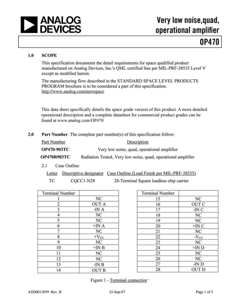
OP470 Very low noise, quad, operational amplifier 3.0 Absolute Maximum Ratings 1/ Supply Voltage (VCC) ......................................................... Differential Input Voltage 2/............................................... Differential Input Current 2/ ............................................... Input Voltage ...................................................................... Output Short Circuit Duration ............................................ Storage Temperature Range................................................ Lead Temperature (soldering, 60 seconds)......................... Power Dissipation (PD) ....................................................... Maximum Junction Temperature (TJ)................................. Ambient Operating Temperature Range............................. ±18V dc ±1V dc ±25mA Supply voltage Continuous -65°C to +150°C +300°C 500mW +150°C -55°C to +125°C Absolute Maximum Ratings Notes: 1/ 2/ 3.1 Stresses above the absolute maximum rating may cause permanent damage to the device. Extended operation at the maximum levels may degrade performance and affect reliability. The inputs are protected by back-to-back diodes. Current limiting resistors are not used in order to achieve low noise performance. If the differential input voltage exceeds ±1V, the input current should be limited to ±25mA. Thermal Characteristics: Thermal Resistance, Lead Leadless Chip Carrier (TC) Package Junction-to-Case (ΘJC) = See MIL-STD-1835 Junction-to-Ambient (ΘJA) = 110 °C/W Max 4.0 Electrical Table: Table I - Electrical Characteristics Parameter Symbol Input Offset Voltage VIO Conditions 1/ M, D, L, R Input Offset Current IIO VCM = 0V M, D, L, R Input Bias Current Input Noise Voltage 4/ IIB En VCM = 0V M, D, L, R fo = 1Hz to 100Hz VO = ±10V, RL = 10kΩ Large Signal Voltage Gain AVS M, D, L, R VO = ±10V, RL = 2kΩ 4/ ASD0013059 Rev. B 25-Sep-07 Subgroups 1 2, 3 1 1 2, 3 1 1 2, 3 1 7 4 5, 6 4 4 5, 6 Limit Min 1000 750 100 500 400 Limit Max ±0.4 ±0.6 ±0.6 ±10 ±20 ±50 ±25 ±50 ±500 110 Units mV nA nVRMS V/mV Page 2 of 5 OP470 Very low noise, quad, operational amplifier Table I - Electrical Characteristics (continued) Conditions Sub1/ groups Output Voltage Swing 4/ VOP RL = 2Kohm 4, 5, 6, No Load 1, 2, 3 Supply Current 2/ ISY M, D, L, R 1 Input Voltage Range 4/ IVR 1, 2, 3 Slew Rate 4/ SR 7 AVLC = +21, RL = 10kΩ 1 Common Mode Rejection 4/ CMR VCM = IVR 3/ 2, 3 1 Power Supply Rejection PSRR VS = ±4.5V to ±18V Ratio 4/ 2, 3 Parameter Symbol Limit Min ±12 Limit Max Units V 11 11 ±11 1.4 110 100 mA V V/μV dB 1.8 5.6 μV/V Table I Notes: 1/ VS = ±15V, RS = 50Ω, unless otherwise specified. 2/ ISY limit equals the total of all four amplifiers. 3/ IVR is defined as the VCM range used for the CMR test. 4/ Not tested Post Irradiation. 4.1 Electrical Test Requirements: Table II Subgroups (in accordance with MIL-PRF-38535, Table III) Test Requirements Interim Electrical Parameters 1 Final Electrical Parameters 1, 2, 3, 4, 5, 6 1/ 2/ Group A Test Requirements 1, 2, 3, 4, 5, 6, 7 Group C end-point electrical parameters 1, 2, 3 2/ Group D end-point electrical parameters 1 Group E end-point electrical parameters 1 1/ PDA applies to Subgroup 1 only. Delta's excluded from PDA. 2/ See Table III for delta parameters. See table I for conditions. 4.2 Life Test and Burn-In Delta Limits: Table III TEST TITLE BURN-IN ENDPOINT LIFETEST ENDPOINT DELTA LIMIT UNITS VIO ±0.4 ±0.5 ±0.1 mV IIB ±25 ±30 ±5 nA IIO ±10 ±15 ±5 nA ASD0013059 Rev. B 25-Sep-07 Page 3 of 5 OP470 Very low noise, quad, operational amplifier 5.0 Life Test/Burn-In Information 5.1 5.2 5.3 HTRB is not applicable for this drawing. Burn-in is per MIL-STD-883 Method 1015 test condition B. Steady state life test is per MIL-STD-883 Method 1005. ASD0013059 Rev. B 25-Sep-07 Page 4 of 5 OP470 Very low noise, quad, operational amplifier Rev A B Description of Change Initiate Update web address. Remove BI circuit. ASD0013059 Rev. B 25-Sep-07 Date Dec. 10, 2002 May 29, 2003 Page 5 of 5
